Skip to the main content.

Join Our Team

We're actively recruiting for a range of roles across sales, engineering, IT and warehouse. Check our careers page to see open positions including apprenticeships. 

View Jobs →

Apprentice_1


Move complex, business-critical equipment

Whether you’re moving a single piece of equipment or an entire production line, our trusted team of engineers can support every step of your move, from rigging to end-to-end relocation support across the globe.

Download Brochure →

Equipment_Move_In_Cleanroom_Flexi_Card


Trusted Partners for the Microelectronics Industry


At IES, we provide our UK, Ireland & Scandinavian customers with Sales, Process & Service Support for a selection of leading International Equipment Manufacturers. These partner companies supply Equipment & Process Development for a range of applications in the Semiconductor, MEMS and Photonics industries. In addition to supporting our Business Partners products, IES also provide cross-trained Process & Service Support for all products for European microelectronic fabrication & R &D facilities resulting in high uptimes and significant operational cost reductions.

EV Group
Metrology
EM Resist
20
Veeco
Savannah
Atomic Layer Deposition
EV Group
Bonding
EV Group
Bonding
EVG®805
805
scia Systems
Metal Deposition
scia Multi 680
680
Fiji
Veeco
Atomic Layer Deposition
EV Group
Bonding
BONDSCALE
EV Group
Nanoimprint Lithography
EVG®510 HE
EV Group
Bonding
EVG®540
EV Group
EVG®50
Metrology
EV Group
Lithography
EVG®105
105
EV Group
Bonding
EVG®810 LT
810
EV Group
Bonding
EVG®560
560
EVG®7200 LA
EV Group
Nanoimprint Lithography
EVG®620 NT
EV Group
Lithography
620
Nanolithography
scia Magna 200
scia Systems
Metal Deposition
200
ComBond
EV Group
Bonding
scia Systems
Chemical Vapour Deposition
scia Cube 300/750
EVG®610 BA
EV Group
Bonding
610
scia Systems
Ion Beam Technology
scia Mill 150
EV Group
Nanoimprint Lithography
EVG®720
720
EV Group
Bonding
EVG®520 IS
scia Coat 500
scia Systems
Ion Beam Technology
EV Group
Bonding
EVG®850 DB
850
EVG®820
EV Group
Bonding
Alpha Plasma
Plasma Etch
Q240 Microwave Plasma Etcher
EV Group
Lithography
HERCULES
scia Systems
Chemical Vapour Deposition
scia Batch 350
350
EV Group
HERCULES NIL
Nanoimprint Lithography
EV Group
Bonding
EVG®850 LT
850
EV Group
Bonding
EVG®620 BA
620
EV Group
Lithography
EVG®610
610
EV Group
Bonding
SmartView NT
EV Group
Bonding
EVG®510
510
scia Systems
Plasma Treatment
scia Clean 1500
Alpha Plasma
Astro 96
Plasma Treatment
IQ ALIGNER
EV Group
Lithography
EV Group
Lithography
IQ ALIGNER NT
AL76/AL76 Compact for Packaging Applications
Alpha Plasma
Plasma Treatment
AL76/AL76
EV Group
Bonding
EVG®850 TB
850
Solaris 150
Surface Science Integration
Rapid Thermal Processing
Alpha Plasma
Plasma Etch
Q235 Microwave Plasma Etcher
235
Q235
EV Group
Lithography
EVG®6200 NT
6200
Firebird
Veeco
Atomic Layer Deposition
EVG®320
EV Group
Bonding
scia Systems
Ion Beam Technology
scia Coat 200
200
EVG®6200 BA
EV Group
Bonding
6200
Lithography
EV Group
EVG®120
120
Alpha Plasma
Plasma Treatment
AL18 Microwave Plasma Etcher System
AL18
EV Group
Bonding
GEMINI FB XT
EVG®501
EV Group
Bonding
AL140 Compact Microwave Plasma Etcher
Alpha Plasma
Plasma Treatment
AL140
EV Group
Lithography
EVG®150
Veeco
Atomic Layer Deposition
Phoenix
EVG®101
EV Group
Lithography
Alpha Plasma
Plasma Etch
Q150 Microwave Plasma Etcher
150
Q150
EV Group
Nanoimprint Lithography
EVG®520 HE
520
scia Mill 200
scia Systems
Ion Beam Technology
200
EV Group
Nanoimprint Lithography
EVG®770
EV Group
Nanoimprint Lithography
EVG®7200
EV Group
Bonding
GEMINI
EV Group
EVG®40 NT
Metrology
40

Technologies


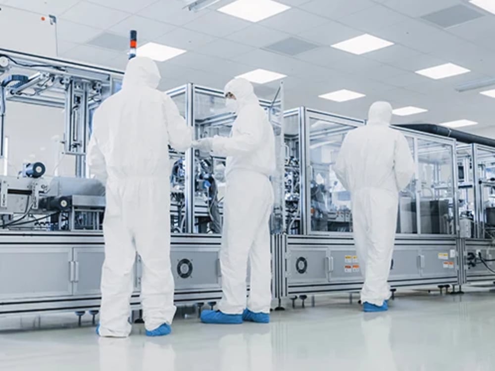
Looking for Advanced R&D or Production Equipment?

IES partners with leading global manufacturers to supply a comprehensive portfolio of process technologies for microelectronics and semiconductor applications. Our offering spans lithography, wafer bonding, resist processing, rapid thermal processing, magnetron & ion beam sputtering, atomic layer deposition, ion beam etching & trimming, resist ashing, surface treatment and parylene deposition. Whether you're working in research, pilot-scale development, or full-scale production, we can help you identify the right tools to meet your process requirements—with expert support throughout the equipment lifecycle.

Need Experienced Field Service or Process Support?

With over three decades of industry experience, IES provides expert field service and applications support across a wide range of semiconductor processing technologies. Our team of highly skilled Field Service and Process Engineers supports key areas including ion implantation, diffusion and LPCVD, epitaxial growth, photolithography, plasma processing, CMP, copper deposition, wafer inspection, and metrology.

Whether you're maintaining legacy tools or optimising new process equipment, we deliver reliable, responsive support tailored to your operational needs.

Seeking New Technology Partners?

IES is actively looking to expand its portfolio by partnering with equipment manufacturers specialising in wet benches, furnaces, plasma etch, electrochemical or atomic layer deposition solutions. We mainly focus on front-end technologies but also have experience in packaging, wafer inspection and metrology. If you are a technology provider looking for experienced representation and support across the UK and Europe, we would welcome the opportunity to discuss how we can work together.

How Can We Help?

Home-Sectors-Semiconductor

Seeking R&D or Semiconductor Production Equipment?

Seeking R&D or Semiconductor Production Equipment? IES represents many equipment suppliers offering a broad range of technologies including e-beam lithography, rapid thermal processing, thermal evaporation, chemical & physical vapour deposition, RF & microwave plasma etch, Atomic Layer Deposition, Cleaving & Scribing and ashing, plasma treatment, ion beam etch & deposition, and parylene deposition for microelectronics processing.

Our Partners

 
Home-Sectors-Semiconductor

Continually adding Principals to meet our customers’ needs

We are seeking Principals supplying the following Equipment:- Scribe/Cleave, Furnaces, Sputtering, Electro-Chemical & Atomic layer Deposition for both Production & Research & Development in the Semiconductor/Nano-technology field.

Products


EVG®20

Savannah

EVG®301

EVG®805

scia Multi 680

Fiji

BONDSCALE

EVG®510 HE

EVG®540

EVG®50

EVG®105

EVG®810 LT

EVG®560

EVG®7200 LA

EVG®620 NT

scia Magna 200

ComBond

scia Cube 300/750

EVG®610 BA

scia Mill 150

EVG®720

EVG®520 IS

scia Coat 500

EVG®850 DB

EVG®820

Q240 Microwave Plasma Etcher

HERCULES

scia Batch 350

HERCULES NIL

EVG®850 LT

EVG®620 BA

EVG®610

SmartView NT

EVG®510

scia Clean 1500

Astro 96

IQ ALIGNER

IQ ALIGNER NT

AL76/AL76 Compact for Packaging Applications

EVG®850 TB

Solaris 150

Q235 Microwave Plasma Etcher

EVG®6200 NT

Firebird

EVG®320

scia Coat 200

EVG®6200 BA

EVG®120

AL18 Microwave Plasma Etcher System

GEMINI FB XT

EVG®501

AL140 Compact Microwave Plasma Etcher

EVG®150

Phoenix

EVG®101

Q150 Microwave Plasma Etcher

EVG®520 HE

scia Mill 200

EVG®770

EVG®7200

GEMINI

EVG®40 NT

EVG®620 NT.

Solaris 200

Experience the Technology Firsthand

Discover the capabilities of our equipment partners — including EVG, scia Systems, Veeco, Alpha plasma and SSI — through live or online demonstrations from their dedicated application labs across Europe and the US. Whether you're exploring a specific process or evaluating a full solution, we can arrange tailored demos to match your requirements.