




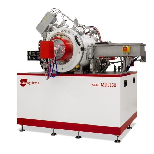
scia Mill 150
What is the scia Mill 150?
The scia Mill 150 is an ion beam etching (IBE) and milling system designed for structuring complex multilayers of various materials, handling single substrates up to 150 mm diameter, loaded via an automatic handling system. IES is the official UK representative for scia Systems, supplying, installing, and supporting the scia Mill 150 for customers across the UK.
What etching processes does it support?
With full reactive gas compatibility, the scia Mill 150 enables Ion Beam Etching (IBE) with inert gases, as well as Reactive Ion Beam Etching (RIBE) and Chemically Assisted Ion Beam Etching (CAIBE), delivering enhanced selectivity and etch rate for reactive processes.
What substrate handling features does it offer?
The substrate holder has helium backside cooling and can be tilted and rotated, giving control over etch angle. Typical applications include structuring metal films for MEMS and sensors.
Why is it suited to R&D and low-volume production?
Its space-saving design makes the scia Mill 150 ideal for small-scale production and R&D applications, where a compact, flexible etching platform is more practical than a full high-volume manufacturing cluster tool.
Where can I buy or get support for the scia Mill 150 in the UK?
As the official UK representative for scia Systems, IES provides UK-based sales, installation, and engineering support for the scia Mill 150 and the wider scia Systems ion beam technology portfolio.
Key Features:
- Etching angle adjustment with tiltable and rotatable substrate holder
- Excellent uniformity without shaper
- Enhanced selectivity and rate with reactive gases
- Process control with exact SIMS based or optical end point detection
- Carrier concept for adaptation to variable substrate sizes
- Processing of wafers with photoresist masks due to good wafer cooling
Technical Data:
- Substrate size (up to) 150 mm dia.
- Substrate holder - Water-cooled, helium backside cooling contact,
substrate rotation 1 to 20 rpm, tiltable in-situ from 0° to 165° in 0.1° steps - Ion beam source - 190 mm circular microwave ECR source (MW218-e)
- Neutralizer - Triple plasma bridge neutralizer (N-3DC)
RF plasma bridge neutralizer (RF-PBN) - Typical removal rates - SiO2: 20 nm/min (inert), SiO2: 40 - 60 nm/min (reactive)
- Uniformity variation - ≤ 3 % (σ/mean)
- Base pressure - < 5 x 10⁻⁷ mbar
- System dimension
(W x D x H)
1.90 m x 1.80 m x 1.75 m
(without electrical rack) - Configurations - Single chamber, optional single substrate load lock,
optional OES or SIMS based end point detection - Software interfaces - SECS II / GEM, OPC
Applications:
- Sensor manufacturing (magnetic, piezoelectric, infrared)
- MEMS fabrication (metal structures, micro-actuators)
- Photonics / optics (gratings, surface relief, optoelectronic microstructures)
- Semiconductor R&D (compound semiconductors, thin film stacks)
- Prototyping / small volume production where high precision etch/milling is required