Expert Engineering Support for Semiconductor Tools
Get a turnkey engineering service you can rely on
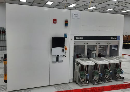
From implanters and furnaces to lithography and bonding systems, we’ve been working with complex semiconductor tools in fabs and cleanrooms all over the world for 35+ years.
Whether you need a single-tool installation, a full production line relocation, or emergency/contracted tool support, our engineers have the expertise, resources and global reach to deliver.
-
Start-to-finish relocation partner for production-critical tools
-
Cleanroom equipment specialist
-
Worldwide support
Partnerships
Areas we support
We support a full spectrum of semiconductor fab equipment, with experienced engineers matched to your specific needs via our Skills Matrix.
Our turnkey relocation service
As part of our turnkey relocation service, we cover every part of your project in-house.
Comprehensive site surveys, method statements and risk assessments
Tool move-out
Tool move-in
Decontamination
Assembly and start-up
Tool dismantling and de-installation
Door-to-door freighting, including customs
Final tests
Shipping brackets/lockdown kit
Support services
We provide a comprehensive range of support services to keep your equipment running at peak performance.
Field service support, including:
-
Emergency tool-down support
-
Short- or long-term contract-based support
-
Bespoke training
Compliance testing, including:
-
UKCA/CE marking
-
PUWER assessments
-
EMF testing
Upgrades
Parts sourcing and provisioning
Trusted by Microchip, Analog Devices, Nexperia and more
We've supported both manufacturers and end users to move, install and commission semiconductor tools since 1991, and have strong working relationships with many world-class microelectronics manufacturers.
![]()
“IES are reliable, flexible, and knowledgeable of the semiconductor industry, so were the best partner for the installation project.”
- Chief Operating Officer, Plessey Semiconductors
Why IES?
-
Proven track record
We have over 35 years of experience working with semiconductor tools in fabs and cleanrooms across the globe.
-
Best-in-class engineers
Our experienced field service engineers have deep expertise working with hundreds of semiconductor tools, processes and manufacturers.
-
Specialist skills matching
We use our Skills Matrix to match you with the most qualified engineers for your equipment, processes and project.
-
Service you can rely on
You get a start-to-finish, end-to-end support service that you can rely on, with no surprises.
-
Standards and specifications
Meet SEMI standards and OEM specifications while delivering your project.
-
Worldwide service
Get the support you need wherever you are, with our worldwide service.
Speak with one of our experts
Request a callback from one of our team or book a site survey for your project.


