




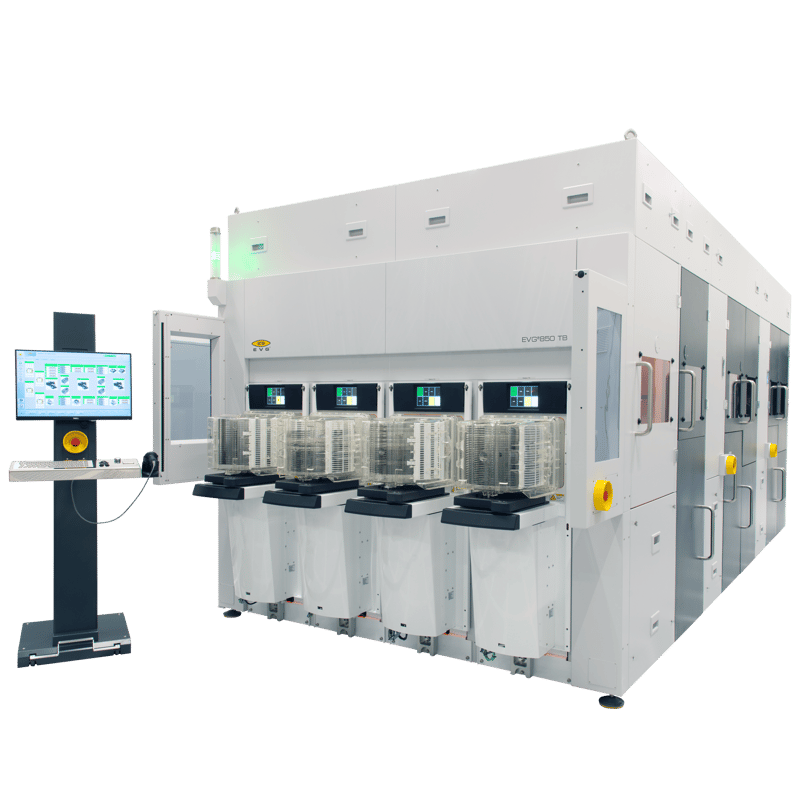
EVG®850 TB
What is the EVG®850 TB?
The EVG®850 TB is a fully automated temporary bonding system that streamlines the entire temporary bonding process — from adhesive application and baking to alignment and bonding of the device wafer to the carrier wafer — all within a single automated tool.
IES is the official UK representative for EV Group (EVG), supplying, installing, and supporting the EVG®850 TB for customers across the UK.
How is the EVG®850 TB's layout designed?
Featuring a modular layout, consistent with all EVG's fully automated tools, the system can be throughput-optimised based on specific process needs — from lower-volume R&D use through to high-throughput production.
What temporary bonding adhesives does the EVG®850 TB support?
Thanks to EVG's open platform design, the system supports a variety of temporary bonding adhesives, including:
Spin-coat thermoplastics
Thermoset materials
Tapes
Where can I buy or get support for the EVG®850 TB in the UK?
As EV Group's official UK representative, IES provides UK-based sales, installation, and engineering support for the EVG®850 TB and the wider EVG temporary bonding portfolio.
Features:
- Open adhesive platform
- Various carriers (silicon, glass, sapphire, etc…)
- Bridge tool capability for different substrate sizes
- Available with multiple load port options and combinations
- Recipe controlled system
- Real time monitoring and recording of all relevant process parameters
- Fully integrated SECS/GEM interface
- Optional integrated inline metrology module for automated feedback loop
Applications:
- Thin-Wafer Processing / Backside Processing
For wafers that need to be thinned, backside etched, or otherwise processed, the temporary bonding to a robust carrier gives mechanical support during those fragile steps. - 3D IC / TSV Integration
In 3D stacking or through-silicon-via (TSV) processes, temporary bonding is often needed to maintain wafer integrity while interconnects are formed, and then debonding is done later.
- MEMS / Sensor Fabrication
MEMS devices with fragile membranes or features benefit from bonding to carrier while backside or postprocessing is done. - Heterogeneous Integration
When combining different types of substrates or materials, temporary bonding helps ensure that processing steps do not damage delicate layers. - Process Development / R&D
The flexibility (open adhesive platform, modular design) means researchers/developers can test different adhesive chemistries, bonding recipes, and carriers. - High-Yield / High-Quality Thin Wafer Flows
The optional inline metrology allows monitoring of key parameters (e.g. adhesive thickness uniformity, voids, warp) to reduce defects and wafer breakage.