




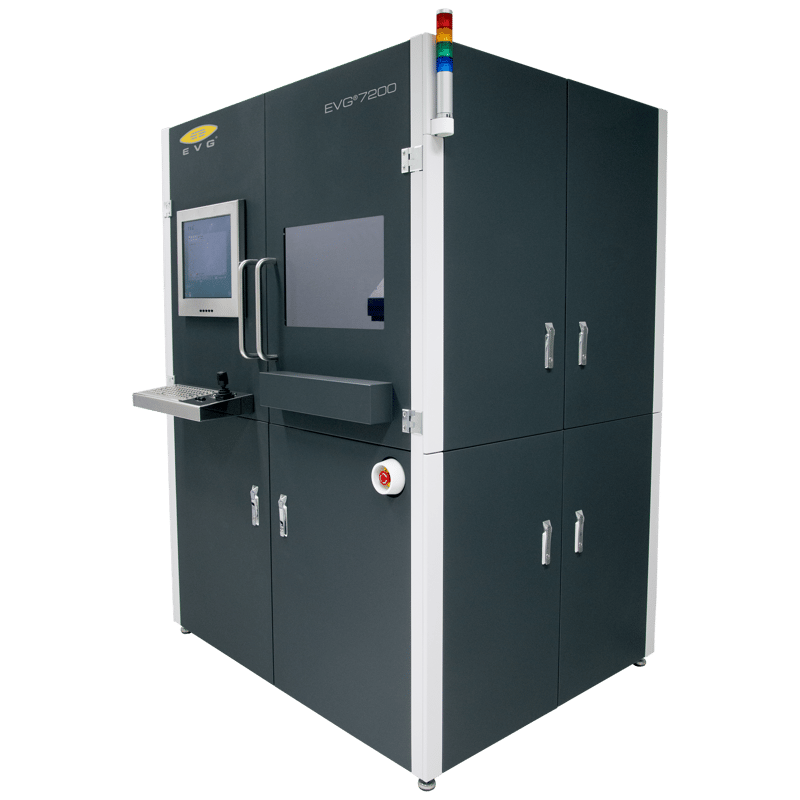
EVG®720
What is the EVG®720?
The EVG®720 incorporates EVG's SmartNIL™ technology, enabling manufacturing of micro- and nanostructures with high pattern fidelity and minimal residual layer. It's available in manual or automated configuration, with automated cassette-to-cassette handling plus a semi-automated R&D mode, supporting substrate sizes from small pieces up to 150 mm. IES is the official UK representative for EV Group (EVG), supplying, installing, and supporting the EVG®720 for customers across the UK.
How does it achieve fast, high-yield imprinting?
Exposure is achieved using tunable intensity LED lamps, giving fast solidification of a wide range of UV-curable materials and significantly improving throughput. Controlled and smooth demolding, supported by force measurement, ensures high yield and precision throughout the process. The system uses multiple-use polymer stamp technology, with integrated imprinting, UV curing, demolding, and working stamp fabrication in one platform.
What can it be used to manufacture?
The EVG®720 prints large-area nanostructures with high throughput, making it suited to high-volume production of next-generation microfluidic and photonic devices, including diffractive optical elements (DOEs). The platform is open to all commercially available imprint materials and scales from R&D through to production.
How does it keep cost of ownership low?
Designed for low cost of ownership and high efficiency, the EVG®720's multiple-use stamp technology and system housing for process stability make it a practical choice for scaling nanoimprint lithography into production.
Where can I buy or get support for the EVG®720 in the UK?
As EV Group's official UK representative, IES provides UK-based sales, installation, and engineering support for the EVG®720 and the wider EVG nanoimprint lithography portfolio.
*Resolution is dependent on process and template.
Features:
- Volume-proven imprinting technology with superior replication fidelity
- Proprietary SmartNIL® technology with multiple-use polymer stamp technology
- Integrated imprinting, UV curing demolding, and working stamp fabrication
- Automated cassette-to-cassette handling plus semi-automated R&D mode
- Optional top-side alignment
- Optional mini-environment
- Open platform for all commercially available imprint materials
- Scalability from R&D to production
- System housing for best process stability and reliability
Applications:
- Diffractive Optical Elements (DOEs) / Optics / Photonics
Manufacturing periodic or quasi‑periodic nanoscale structures for wavefront shaping, gratings, beam splitting, diffractive lenses, optical filters. The full-field imprint and high fidelity make it appropriate. - Microfluidics / Lab-on-a-Chip
Imprinting micro- and nanoscale channels, features, surface textures in polymer layers; useful due to its ability to pattern large areas and conform to non-ideal surfaces. - Meta-surfaces / Metastructures / Nanophotonics
Creating arrays of sub‑wavelength features for manipulating light (e.g. metasurfaces for lenses, beam steering, color, polarization). - Bio‑/Medical Devices
Patterning of nano-/micro‑structured surfaces for cell interaction, bio-sensing surfaces, micro‑arrays, etc. - Micro- & Nano-Optics for AR/VR / Waveguides
Imprinting optical waveguides or surface diffractive structures used in displays, augmented reality devices, micro‑optical elements. - Prototype / Pilot Production of Nanopatterned Surfaces
Because the EVG 720 supports automation and throughput, it is useful not only for R&D but also small volume manufacturing of devices requiring nano-scale patterning. - High Throughput Nanopatterning
The integration of imprinting + curing + demolding enables continuous or semi-continuous workflows, reducing handling steps and increasing throughput.