




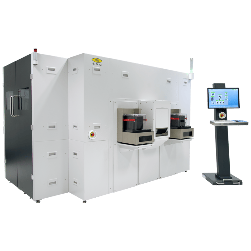
EVG®850 DB
What is the EVG®850 DB?
The EVG®850 DB is a fully automated debonder designed for the separation and cleaning of processed temporary bonding wafer stacks. IES is the official UK representative for EV Group (EVG), supplying, installing, and supporting the EVG®850 DB for customers across the UK.
How are fragile device wafers supported during debonding?
To ensure the fragile device wafers remain securely supported throughout the process, they are mounted either via film frame or handled using a thin wafer handler.
Where can I buy or get support for the EVG®850 DB in the UK?
As EV Group's official UK representative, IES provides UK-based sales, installation, and engineering support for the EVG®850 DB and the wider EVG temporary bonding and debonding portfolio.
Features:
- Reliable handling of thinned, bowed and warped wafers with and without topography
- Automated cleaning of debonded wafer
- Recipe controlled system
- Real time monitoring and recording of all relevant process parameters
- Fully integrated SECS/GEM interface in automated tools
- Bridge tool capability for different substrate sizes
- Modular tool layout → throughput-optimized depending on specific process
Applications:
- Temporary bonding / debond workflows
In processes where a device wafer is bonded to a carrier temporarily (for thinning, backside processing, etc.), the 850 DB is used to safely separate them after processing. - 3D integration, TSV, advanced packaging
In 3D ICs or through-silicon via (TSV) processes, wafers are often thinned and require support. After backend steps, debonding is critical. - MEMS / thin-device processing
MEMS devices, sensors, or devices with fragile membranes benefit from a gentle, controlled debonding process. - Power / compound semiconductor devices
For high-voltage or compound semiconductor devices, thinning and backside operations are common; having a reliable debonder helps protect yield. - High‑throughput / production environment
The fully automated nature, integrated cleaning, and wafer handling make 850 DB suitable for volume or pilot manufacturing of devices using thin-wafer flows. - Process development & R&D
Because it supports multiple debond modalities and real-time monitoring, it is useful for testing new adhesive materials, debond recipes, and process optimization in a lab or pilot setting.