




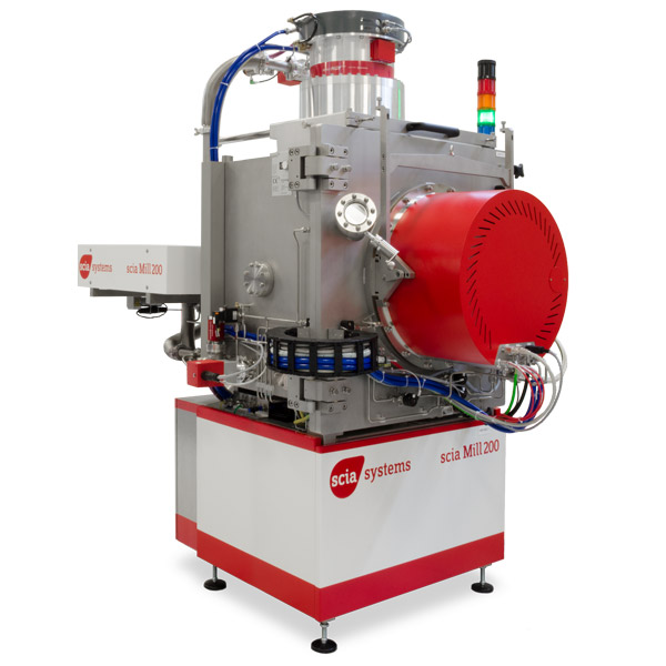
scia Mill 200
What is the scia Mill 200?
The scia Mill 200 is an ion beam etching and milling system designed for structuring complex multilayers of various materials, handling wafers up to 200 mm diameter with an automatic handling system for loading wafers and carriers. IES is an equipment partner for scia Systems, supplying, installing, and supporting the scia Mill 200 for customers across the UK.
How does it enable precise process control?
The scia Mill 200 offers precise process control with customisable endpoint detection systems, including optional SIMS end point detection for recognition of etched species and a defined etch stop — useful for applications where contamination must stay very low.
What etching processes does it support?
Featuring full reactive gas compatibility, the system enables reactive etching processes with enhanced selectivity and rate, and is typically used for Reactive Ion Beam Etching (RIBE), Ion Beam Etching (IBE) with inert gases, and Chemically Assisted Ion Beam Etching (CAIBE). The system can also be upgraded for Dual Ion Beam Deposition (DIBD) with an additional target holder and ion beam sputter source.
How does it scale from R&D to high-volume production?
Its flexible design allows adaptation for both single-substrate applications and high-volume production cluster configurations, with up to three process chambers and two cassette load locks — letting the same underlying platform support both lab-scale and production environments.
Where can I buy or get support for the scia Mill 200 in the UK?
As an equipment partner for scia Systems, IES provides UK-based sales, installation, and engineering support for the scia Mill 200 and the wider scia Systems ion beam technology portfolio.
Key Features:
- Etching angle adjustment with tiltable and rotatable substrate holder
- Excellent uniformity without shaper
- Enhanced selectivity and rate with reactive gases
- Process control with exact SIMS based or optical end point detection
- Processing of wafers with photoresist masks due to good wafer cooling
- Fully automatic cassette handling in variable cluster layouts including SECS/GEM
communication
Technical Data:
- Substrate size (up to) - 200 mm dia.
- Substrate holder - Water-cooled, helium backside cooling contact, substrate
rotation 1 to 20 rpm, tiltable in-situ from 0° to 170° in 0.1° steps - Ion beam source - 350 mm circular RF source (RF350-e)
- Neutralizer - RF plasma bridge neutralizer (N-RF)
- Typical removal rates - Cu: 60 nm/min, Pt: 35 nm/min, W:18 nm/min,
SiO2: 20 nm/min (inert), SiO2: 40 - 60 nm/min (reactive) - Uniformity variation - ≤ 1 % (σ/mean)
- Throughput - 12 Wafer/h (100 nm SiO2 on 200 mm wafer)
- Base pressure - < 5 x 10⁻⁷ mbar
- System dimension -
(W x D x H)
3.20 m x 2.50 m x 2.50 m, for 3 chambers and cassette handling
(without electrical racks and pumps) - Configurations - Single chamber, optional single substrate load lock
or cassette handling, cluster system with up to 3 process
chambers and cassette handling, optional OES or SIMS based
end point detection - Software interfaces - SECS II / GEM, OPC
Applications:
- Spintronics / Magnetic sensors:
Etching TMR or GMR stacks with precise layer control to achieve correct functionality. E.g., etching at different angles and monitoring by SIMS. - MEMS and micro-devices:
Milling of metal/dielectric stacks to form electrodes, micro-actuators, or MEMS structures. - Optoelectronics / Photonics:
Fabrication of optical gratings, waveguides, surface relief elements for AR/MR applications, or integrated photonic circuits. - Wide-bandgap power electronics:
Etching of GaN, SiC based devices where conventional etch technologies are less effective, taking advantage of reactive ion-beam capability. - Sensor manufacturing: For instance ultra-thin LiTaO₃ for IR sensors, or other compound substrates needing precise thinning, smoothing or structure formation.