




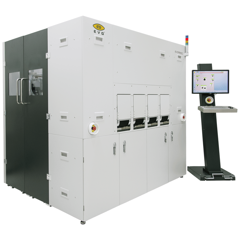
EVG®850 LT
What is the EVG®850 LT?
Wafer bonding is a critical enabling technology for SOI wafer fabrication and wafer-level 3D integration. The EVG®850 LT is an automated production bonding system for mechanically aligned SOI and direct wafer bonding, using LowTemp™ plasma activation, with 300mm capability.
IES is the official UK representative for EV Group (EVG), supplying, installing, and supporting the EVG®850 LT for customers across the UK.
How does it streamline the fusion bonding process?
The EVG®850 LT combines all essential steps for fusion bonding — cleaning, plasma activation and alignment, pre-bonding, and IR inspection — in a single system, with automated cassette-to-cassette operation (ergo load, SMIF, or FOUP). This makes it a key enabler for SOI wafer fabrication and wafer-level 3D integration.
What results does it deliver in production environments?
Field-proven and established as an industry standard, the EVG®850 LT is a production system built to operate in high-throughput, high-yield environments, delivering void-free bonds for reliable results across a wide range of fusion/molecular wafer bonding applications.
Where can I buy or get support for the EVG®850 LT in the UK?
As EV Group's official UK representative, IES provides UK-based sales, installation, and engineering support for the EVG®850 LT and the wider EVG bonding equipment portfolio.
Features:
- SOI and direct wafer bonding with EVG's LowTemp™ plasma activation
- Suitable for a wide range of fusion/molecular wafer bonding applications
- Production system built to operate in high-throughput, high-yield environments
- Automated cassette-to-cassette operation (ergo load, SMIF or FOUP)
- Contamination-free backside handling
- Megasonic and/or brush cleaning
- Pre-bonding with mechanical flat or notch alignment Advanced remote diagnostics
Applications:
- Silicon-on-Insulator (SOI) Wafer Fabrication
The EVG®850 LT is instrumental in producing SOI wafers by bonding a thin silicon layer onto an insulating substrate, a process vital for advanced semiconductor devices. - Direct Wafer Bonding
Facilitates direct bonding of wafers without the need for intermediate adhesives, enabling the creation of engineered substrates and layer transfer applications. - 3D Wafer-Level Integration
Supports wafer-level 3D integration by enabling the bonding of multiple wafer layers, essential for advanced packaging and heterogeneous integration. - Backside Illuminated (BSI) CMOS Image Sensors
Enables the fabrication of BSI CMOS image sensors by bonding wafers with precise alignment, enhancing the performance of imaging devices. - Advanced Substrate Bonding
Applicable in bonding various advanced substrates, including compound semiconductors and MEMS devices, for the development of next-generation electronic and photonic systems.