




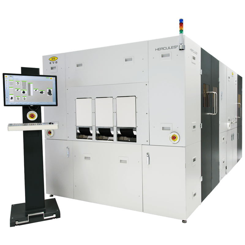
HERCULES
What is the HERCULES® NIL 200mm?
The HERCULES® NIL 200mm is the industry standard for high-volume nanoimprint lithography, combining EVG's proprietary SmartNIL™ imprinting technology with essential pre-processing steps, including cleaning, resist coating, and baking, on a 200 mm platform.
IES is the official UK representative for EV Group (EVG), supplying, installing, and supporting the HERCULES® NIL 200mm for customers across the UK.
How is it configured for high-volume production?
Built on a modular platform, the system offers tunable configurations that maximise throughput while maintaining a low footprint, giving a cost-effective solution for large-scale production. Advanced handling systems deliver highly efficient processing across the 200 mm platform.
How does it reduce equipment and process overhead?
The HERCULES® NIL 200mm can fabricate multiple-use soft stamps in-line — a critical requirement for high-volume production — without needing separate equipment for imprint stamp manufacturing, keeping the process chain within a single platform.
What applications is it used for?
The system supports a wide range of applications, including optical devices for AR/VR headsets, 3D sensors, biomedical devices, nanophotonics, plasmonics, and metasurfaces, providing a complete NIL solution for high-volume manufacturing.
Where can I buy or get support for the HERCULES® NIL 200mm in the UK?
As EV Group's official UK representative, IES provides UK-based sales, installation, and engineering support for the HERCULES® NIL 200mm and the wider EVG nanoimprint lithography portfolio.
Features:
- Production platform combines all advantages of EVG’s precision alignment and resist processing systems in a minimized footprint
- Versatile platform supports fully automated processing of various substrate shapes, sizes, highly warped mold wafers and even trays
- Coating of up to 52,000 cP enables manufacturing of ultra-thick resist features of up to 300 microns in height
- CoverSpinTM rotating cover for low resist consumption and optimized resist coating uniformity
- OmniSpray® coating for optimized coating of high topography surfaces
- NanoSpray® for coating and protection of via structures Automated mask handling and storage
- Optical edge exposure and/or solvent cleaning for edge bead removal
- Fragile, thin or warped wafer handling of multiple wafer sizes with bridge-tool system
- Rework sorting wafer management and flexible cassette system
- Multi-user concept (unlimited number of user accounts and recipes, assignable access rights, different user interface languages)
Applications:
- Photonics & Optics - Patterning of optical devices: e.g., AR/VR optics, waveguides, nanophotonics, plasmonics. The system supports structures down to ~40 nm and up, including 3D shapes.
- MEMS / NEMS - Micro-electromechanical and nano-electromechanical devices that require fine patterning & high topography handling. Because HERCULES supports warped/thick wafers and high topography surfaces.
- Bio / Biomedical Devices - Devices with micro-/nano-features for biotech applications.The integrated flow helps reduce contamination, improves throughput for specialized wafers.
- Advanced Packaging / Heterogeneous Integration - Patterning of resist layers, coating on non-standard shapes, wafer-level optics etc.
Especially surfaces that are difficult or non-standard (thick, bowed, rectangular). - Nanoimprint Lithography (NIL) variant - In the HERCULES NIL variation: full-area imprinting of nanostructures (anti-reflective layers, color filters, patterned sapphire substrates etc) For example: anti-reflection, light-guiding plates for LEDs & display applications.