




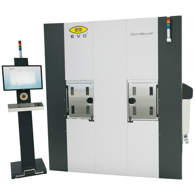
ComBond
What is the EVG® ComBond?
The EVG® ComBond is a high-vacuum wafer bonding platform that sets a new standard in EVG's portfolio, designed to meet the growing demand for advanced integration processes. IES is the official UK representative for EV Group (EVG), supplying, installing, and supporting the EVG® ComBond for customers across the UK.
What applications is the EVG® ComBond used for?
The EVG® ComBond is ideal for a wide range of applications, including:
Engineered substrates
Stacked solar cells
Power devices
High-end MEMS packaging
Beyond-CMOS technologies
How flexible is the EVG® ComBond's design?
Its modular cluster design offers exceptional flexibility, enabling customisation for both R&D and high-throughput, high-volume manufacturing environments — so the same platform can scale from lab-scale development to full production.
How does the EVG® ComBond bond heterogeneous materials?
The platform excels in bonding heterogeneous materials with different lattice constants and coefficients of thermal expansion (CTE). Its unique oxide-removal process enables the formation of electrically conductive bond interfaces, and its high-vacuum technology supports low-temperature bonding of metals such as aluminium, which re-oxidise quickly in ambient environments.
What bond quality can the EVG® ComBond achieve?
Void-free and particle-free bond interfaces, along with exceptional bond strength, can be achieved across a broad range of material combinations, making it suited to advanced device fabrication.
Where can I buy or get support for the EVG® ComBond in the UK?
As EV Group's official UK representative, IES provides UK-based sales, installation, and engineering support for the EVG® ComBond and the wider EVG wafer bonding portfolio.
Features:
- High-vacuum, aligned, covalent bonding
- Processing in high-vacuum environment (< 5·10-8 mbar)
- In-situ sub-micron face-to-face alignment accuracy
- High-vacuum MEMS and optical device encapsulation
- In-situ surface and native oxide removal
- Superior surface properties
- Conductive bonding
- Room-temperature process
- Multiple material combinations, including metals (aluminum)
- Stress-free bond interface
- High bond strength
- Modular system for HVM and R&D
- Flexible configurations up to six modules
- Substrate size up to 200 mm
- Fully automated
Applications:
- “Beyond CMOS” / advanced logic / high-mobility devices
When integrating different semiconductor materials (e.g. III-V on Si), oxide-free bonding via ComBond helps maintain high interface quality. - MEMS / vacuum-sealed MEMS devices
For MEMS requiring vacuum encapsulation (gyroscopes, accelerometers, microbolometers, etc.), ComBond can bond capping wafers under vacuum and maintain high vacuum environments inside. - Power / high-voltage / power electronics
Bonding wide bandgap materials, or bonding heterogenous materials (e.g. SiC, GaN) with minimal thermal damage and strong interfaces, is possible with ComBond.