




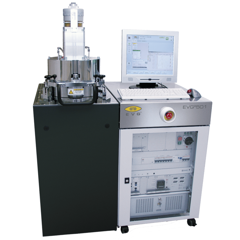
EVG®501
What is the EVG®501?
The EVG®501 is a highly flexible wafer bonding system that supports all common bonding processes — anodic, glass frit, solder, eutectic, transient liquid phase, and direct bonding — in a single tool. IES is the official UK representative for EV Group (EVG), supplying, installing, and supporting the EVG®501 for customers across the UK.
What bonding processes does the EVG®501 support?
The system covers the full range of standard wafer bonding methods, including:
Anodic bonding
Glass frit bonding
Solder bonding
Eutectic bonding
Transient liquid phase bonding
Direct bonding
Who is the EVG®501 designed for?
Its easy-access bond chamber and user-friendly tooling design allow quick retooling between different wafer sizes and processes, making it well suited to universities, R&D facilities, and low-volume production environments where flexibility matters more than raw throughput.
How does the EVG®501 support scale-up to production?
The bond chamber design mirrors that of EVG's high-volume manufacturing tools, such as the EVG® GEMINI, so bonding recipes developed on the EVG®501 transfer directly across. This gives a seamless path from R&D and low-volume work to larger production volumes as requirements grow, without having to redevelop processes from scratch.
Where can I buy or get support for the EVG®501 in the UK?
As EV Group's official UK representative, IES provides UK-based sales, installation, and engineering support for the EVG®501 and the wider EVG wafer bonding portfolio.
Features:
- Unique pressure and temperature uniformity
- Compatible with EVG mechanical and optical aligners
- Flexible design and configurations for research
- From single chips to wafers
- Various processes (eutectic, solder, TLP, direct bonding)
- Optional turbopump (<1E-5mbar)
- Upgradeable for anodic bonding
- Open chamber design for easy conversion and maintenance
- Pilot production compatible
- Open chamber design for easy conversion and maintenance
- Smallest footprint for a 200 mm bonding system: 0.8 m2
- Recipes are fully compatible with EVG’s high-volume-manufacturing bonding systems
Technical Data:
- Max contact force
20 KN - Heater Size
150 mm - single chips
200 mm - 100 mm - Vacuum
Standard: 0.1 mbar
Optional: 1E-5 mbar - Max temperature:
450 °C - Single chips processing
Yes - Bond chuck system / Alignment system
150 mm heater: EVG®610, EVG®620, EVG®6200
200 mm heater: EVG®6200, SmartView® NT - Active Water cooling
For bottom side - Power supply for anodic bonding
Max. voltage: 2 kV
Max. current: 50 mA - Loading chamber
Manual
Applications:
- MEMS and Sensors: Fabrication of micro-electromechanical systems and sensors.
- Optical Devices: Production of waveguides and other optical components.
- 3D Integration: Stacking of chips for 3D integration.
- Advanced Packaging: Packaging of semiconductor devices.
- Research and Development: Development of new bonding processes and materials.