




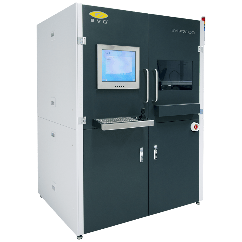
EVG®7200
What is the EVG®7200?
The EVG®7200 uses EVG's advanced SmartNIL™ technology, enabling fabrication of micro- and nanostructures with high pattern fidelity and low residual layer, on substrate sizes from small pieces up to 200 mm — a step up in scale from the 150 mm EVG®720. IES is the official UK representative for EV Group (EVG), supplying, installing, and supporting the EVG®7200 for customers across the UK.
How does it achieve fast, high-yield imprinting?
Exposure is driven by tunable LED lamps, allowing rapid solidification of a wide range of UV-curable materials and improving throughput. The system ensures high yield through controlled, smooth demolding with integrated force measurement for precision. It's built as an open platform compatible with all commercially available imprint materials, and scales from R&D through to production.
What can it be used to manufacture?
Ideal for large-area nanostructure printing, the EVG®7200 delivers high throughput for volume production of next-generation microfluidic and photonic devices, such as diffractive optical elements (DOEs).
How does it keep cost of ownership low?
The EVG®7200 combines high performance with cost efficiency, positioning it as a practical solution for advanced nanotechnology applications moving from development into volume manufacturing.
Where can I buy or get support for the EVG®7200 in the UK?
As EV Group's official UK representative, IES provides UK-based sales, installation, and engineering support for the EVG®7200 and the wider EVG nanoimprint lithography portfolio.
*Resolution is dependent on process and template.
Features:
- Volume-proven imprinting technology with superior replication fidelity
- Proprietary SmartNIL® technology with multiple-use polymer stamp technology
- Integrated imprinting, UV curing, demolding, and working stamp fabrication
- Automated cassette-to-cassette handling plus semi-automated R&D mode
- Optional top-side alignment
- Optional mini-environment
- Open platform for all commercially available imprint materials
- Scalability from R&D to production
- System housing for best process stability and reliability
Applications:
- Display Technologies
Fabrication of wire grid polarizers and other optical components for displays. - Photonic Devices
Production of diffractive optical elements (DOEs) and other photonic structures. - Biotechnology
Development of microfluidic devices and lab-on-a-chip systems. - Optical Components
Manufacturing of micro-optical lenses and gratings.