




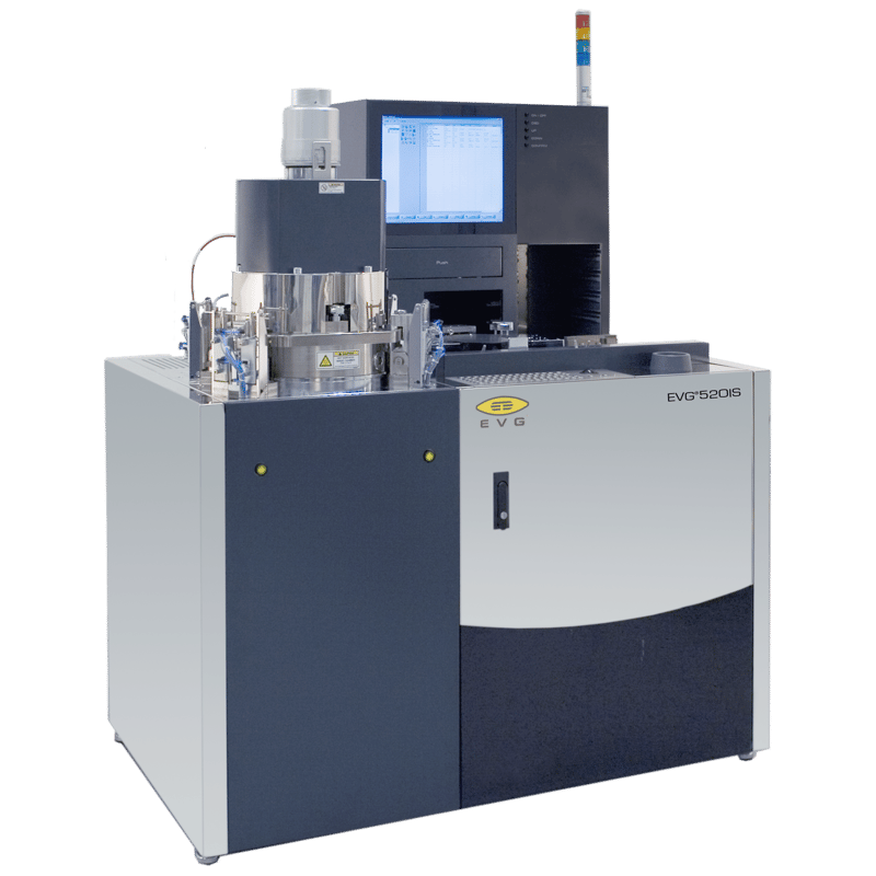
EVG®520 IS
What is the EVG®520 IS?
The EVG®520 IS is a wafer bonding system optimised for small-volume production applications, built on customer feedback and EV Group's continuous technological innovations. IES is the official UK representative for EV Group (EVG), supplying, installing, and supporting the EVG®520 IS for customers across the UK.
What makes the EVG®520 IS's bonding chuck design different?
It features EVG's proprietary symmetric rapid heating and cooling chuck design, which delivers superior temperature and force uniformity across the wafer for more precise, repeatable bonding.
What bonding capability does the EVG®520 IS offer?
The EVG®520 IS provides high-force bonding capability, combined with the same material and process flexibility as manual systems, so it can handle a wide range of wafer bonding processes without being limited to a fixed recipe or material set.
Who is the EVG®520 IS suited for?
It's designed for small-volume production, giving customers a reliable, repeatable bonding platform for diverse production needs without the overhead of a full high-volume manufacturing tool.
Where can I buy or get support for the EVG®520 IS in the UK?
As EV Group's official UK representative, IES provides UK-based sales, installation, and engineering support for the EVG®520 IS and the wider EVG wafer bonding portfolio.
Features:
- Fully automated processing with manual loading and unloading including external cooling station
- Compatible with EVG mechanical and optical aligners
- Single- or double-chamber automated system
- Fully automated bond process execution and bond cover movements
- Integrated cooling station for high throughput
- Options: High vacuum capability (1E-6 mbar) Programmable mass flow controller
- Integrated cooling
Applications:
- MEMS / Microdevices
Bonding microelectromechanical devices (e.g. capping, wafer stacking, chamber sealing) often requires precise temperature control, force, and vacuum. - 3D Integration / Heterogeneous Integration
Bonding dissimilar materials or stacking wafers (e.g. logic + sensor layers) with controlled thermal gradients and high-pressure bonding helps ensure good interface quality. - Optoelectronics / Photonics
Bonding optical wafers (e.g. glass, silicon, transparent substrates) for waveguides, photonic circuits, or substrate bonding in photonic device stacks. - Wafer-Level Packaging
In packaging processes where wafers are bonded before dicing — e.g. sealing, capping, interposer stacking — the EVG 520 IS provides automation and high throughput.