




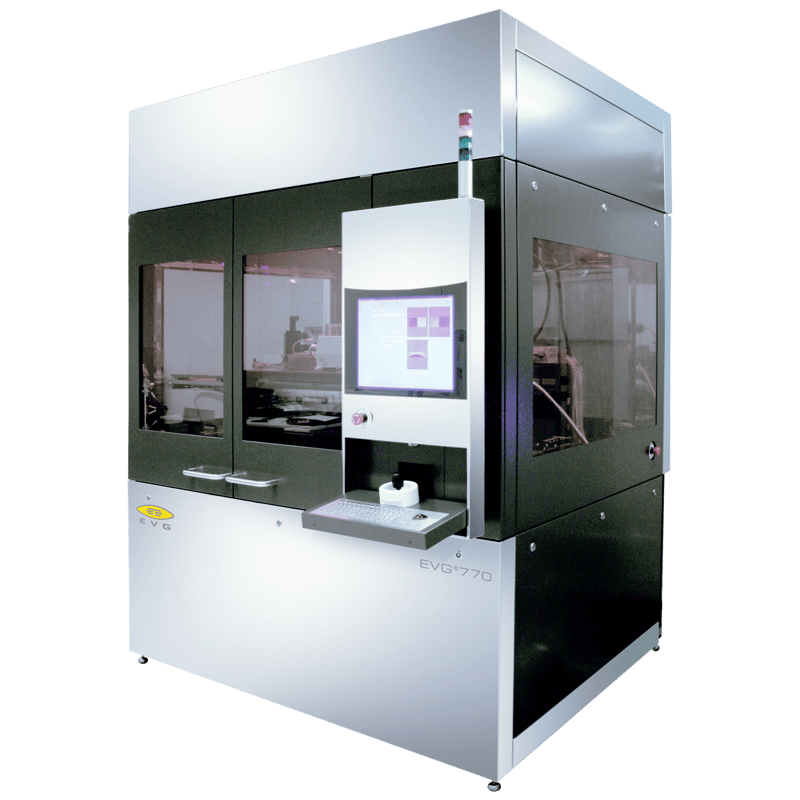
EVG®770
What is the EVG®770 NT?
The EVG®770 NT is a versatile platform for step-and-repeat (S&R) nanoimprint lithography, used for efficient master fabrication or direct patterning of complex structures on substrates. It enables uniform replication of templates from small dies up to 30 cm², and can replicate those dies multiple times over large areas up to Gen 2 panel-size substrates.
IES is the official UK representative for EV Group (EVG), supplying, installing, and supporting the EVG®770 NT for customers across the UK.
How does the step-and-repeat process work?
Often used in conjunction with diamond turning or direct writing methods, the S&R imprinting process is a key step in efficiently fabricating masters required for wafer-level optics manufacturing or EVG's SmartNIL™ process — taking a single die pattern and replicating it precisely across a much larger substrate area.
What applications does it support?
The EVG®770 NT plays a role in high-volume manufacturing of advanced applications, including augmented reality waveguides, optical sensors, diffractive optics, metasurfaces, and biomedical devices.
What process control does it offer?
Key features of the EVG®770 NT include precise alignment capabilities, full process control, and the flexibility to meet the demanding requirements of a range of structures and materials.
Where can I buy or get support for the EVG®770 NT in the UK?
As EV Group's official UK representative, IES provides UK-based sales, installation, and engineering support for the EVG®770 NT and the wider EVG nanoimprint lithography portfolio.
Features:
- Efficient master fabrication of microlenses for wafer-level optics down to nanostructures for SmartNIL®
- Simple implementation of different kind of masters
- Variable resist dispense modes
- Live image during dispensing, imprinting and demolding In-situ force control for imprint and demolding
- Optional optical wedge error compensation
- Optional automated cassette-to-cassette handling
Applications:
- Wafer-Level Optics (WLO): Fabrication of microlenses and other optical components for advanced imaging systems.
- Augmented Reality (AR) Waveguides: Production of waveguides for AR devices, enabling advanced display technologies.
- Diffractive Optics: Manufacturing of diffractive optical elements for various photonic applications.
- Metasurfaces: Creation of nanostructured surfaces with tailored optical properties.
- Biomedical Devices: Development of microfluidic devices and lab-on-a-chip systems for medical diagnostics and research.