


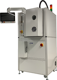
Labcoater Series 300
What is the Labcoater Series 300?
The Labcoater Series 300 is a versatile coating system for laboratory and small-scale production use. Designed for both laboratory environments and production facilities, it's particularly well suited to smaller companies and production teams. IES is an equipment partner for PPS (Plasma Parylene Systems), supplying, installing, and supporting the Labcoater Series 300 for customers across the UK.
What chamber options does it offer?
With four chamber sizes starting at 25 litres, optional equipment, and a built-in plasma source, it adapts seamlessly to your needs. Modular chamber volumes let you match the system to your application, with flexible options starting at 25 L and expandable to 35, 40, or 80 L configurations.
What does the built-in plasma source add?
The Labcoater Series 300 integrates a 2.45 GHz, 600 W plasma source directly into the unit, enabling effective and uniform surface pre-treatment before parylene deposition — helping parylene adhere to difficult substrates such as silicone before coating.
What is it used for?
Applications include implantable electronics such as pacemakers, neurostimulators, and implantable sensors, where parylene forms very conformal, biocompatible films; catheters and microfluidic devices, where plasma pre-treatment aids adhesion to polymers like silicone; medical tools and elastomeric parts such as seals and gaskets, coated for low friction and biocompatibility; and PCBs and MEMS devices, protected from moisture and ionic contamination with high dielectric insulation.Is a cleanroom version available?Yes — the Labcoater Series 300 is also available in a cleanroom version, delivering reliable performance in a compact, versatile design suited to controlled-environment production.Where can I buy or get support for the Labcoater Series 300 in the UK?As an equipment partner for PPS, IES provides UK-based sales, installation, and engineering support for the Labcoater Series 300 and the wider PPS parylene coating portfolio, including the Labcoater Series 100.
Key Features:
- Versatile Laboratory & Small-Scale Production Solution Designed for both laboratory environments and production facilities, this system is particularly well-suited for smaller companies and production teams.
- Built-in Plasma Source for Surface Pre-Treatment Integrates a 2.45 GHz, 600 W plasma source directly into the unit, enabling effective and uniform surface pre-treatment before parylene deposition.
- Modular Chamber Volumes to Match Application Needs Offers flexible options for process chamber volume—starting at 25 L and expandable to 35, 40, or 80 L configurations.
- Detailed Chamber Geometry for Various Capacities
- 25 L: 300 mm diameter × 300 mm height
- 35 L: 300 mm diameter × 350 mm height
- 80 L: 450 mm diameter × 500 mm height
- Advanced Gas Handling Capabilities Includes one gas channel within the chamber, with the flexibility to expand to up to three channels to support diverse process gases.
- Efficient Cooling & Vacuum System Integration Equipped with a 4-liter electromechanical cool-trap for effective condensation management, DIN 40 ISO-KF vacuum connections, an electromagnetic solenoid valve for venting, and a robust 50 m³/h vacuum pump.
- Compact & Sturdy Build
- Dimensions: 1,220 mm (L) × 1,050 mm (W) × 1,920 mm (H)
- Weight: approximately 110 kg
- Flexible Electrical Compatibility
- Operates using 3/N/PE AC power at 50 Hz, compatible with 400 V or 240 V configurations, with a maximum power consumption of 8.5 kW.
- Optional Cleanroom Configuration
Technical Data:
- Dimensions: L: 1220mm W: 1050mm H: 1920mm
- Weight: 110 KG
- Volume: 25 / 35 / 40 / 80 Liter
- Process chamber: 300mm Ø H: 300mm (25 Liter), 300mm Ø / H: 350mm (35 Liter),
- 450mm Ø, H: 500mm (80) Liter
- Plasma source: 2,45GHz, 600 Watt
- Inclusive: 1 gas channel (gas distribution system inside the process chamber), up to 3 channels possible
- Cooling system: 4 liter (electromechanical Cool-trap)
- Vacuum connection: DIN 40 ISO-KF
- Venting: electromagnetic solenoid valve
- Pump system: 50m³/h
- Electrical connection: 3/N/PE AC 50Hz 400 V / 240 V, max. 8.5 KW
Applications:
- Medical & Biomedical Devices Implantable electronics: Because parylene can form very conformal, biocompatible films, the Series 300 could be used for coating pacemakers, neurostimulators, or implantable sensors. Catheters / microfluidics: Plasma pre-treatment helps parylene adhere to difficult polymers (e.g. silicone), so this system is ideal for coating the shafts of catheters, lab-on-chip devices or surgical guides. Medical tools & elastomers: Coating small elastomeric parts (e.g. seals, gaskets) with low friction, biocompatible parylene for use in medical devices.
- Electronics, MEMS, and Sensors Printed Circuit Boards (PCBs): Coating PCBs to protect against moisture, ionic contamination, and to provide high dielectric insulation. MEMS devices: Because parylene is deposited in a molecular / vapour way, it can coat very fine structures, including inside cavities, without damaging delicate MEMS features. Sensors (pressure, gas, RF): For sensors exposed to harsh environments, parylene provides a pinhole-free, conformal barrier. RF / high-frequency components: Low-loss dielectric coatings are possible; plasma activation helps ensure consistent, high-quality insulating films.
- Aerospace, Defence & Harsh Environments Avionics and satellite electronics: Use of parylene to protect from moisture, outgassing, and extreme environmental stresses. Military electronics: Ruggedization of sensitive components (radios, navigation modules, guidance sensors) by using parylene to guard against corrosion and high stress. Industrial / marine sensors: Parylene-coated control boards or sensors operating in corrosive or high-humidity environments.
- Automotive & EV Battery management systems (BMS): Coating of electronics used in EV battery packs, thanks to parylene’s dielectric strength and chemical resistance. Sensors / connectors in under-hood or harsh parts: Parylene helps with moisture, salt, and chemical protection.
- Optics, LEDs, and Display Technologies LED encapsulation: Protecting wire bonds and phosphor regions from moisture with very thin, transparent parylene. Optical assemblies / lenses: Providing protective, chemically inert coatings on optical parts without altering their shape or function.
- Research / Advanced / Nanoscale Devices Flexible / implantable electronics: For example, neural probes or flexible bio-electronic interfaces where adhesion and biocompatibility are critical. Ultra-thin films for nanoscale devices: If using very thin parylene layers (e.g. nanometre-scale), this system could be used for prototyping in research labs. Low-outgassing systems for vacuum / space research: Given parylene’s use in space-grade electronics, a lab-scale coater with plasma pre-treatment could be used for development of space sensors / instrumentation.