




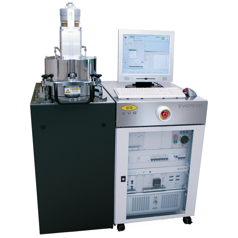
EVG®510
What is the EVG®510?
The EVG®510 is a highly flexible wafer bonding system supporting a wide range of processes, including anodic, glass frit, solder, eutectic, transient liquid phase, and direct bonding. IES is the official UK representative for EV Group (EVG), supplying, installing, and supporting the EVG®510 for customers across the UK.
What bonding processes does the EVG®510 support?
The system covers a wide range of wafer bonding methods, including:
Anodic bonding
Glass frit bonding
Solder bonding
Eutectic bonding
Transient liquid phase bonding
Direct bonding
Who is the EVG®510 designed for?
Its easy-access bond chamber and intuitive tooling design allow quick retooling between different wafer sizes and processes, making it an excellent choice for universities, R&D facilities, and low-volume production applications.
How does the EVG®510 support scale-up to production?
The bond chamber design closely mirrors that of EVG's high-volume manufacturing tools, such as the EVG® GEMINI, ensuring compatibility and enabling easy transfer of bonding recipes. This makes the EVG®510 an ideal platform for scaling up production volumes as needs evolve.
Where can I buy or get support for the EVG®510 in the UK?
As EV Group's official UK representative, IES provides UK-based sales, installation, and engineering support for the EVG®510 and the wider EVG wafer bonding portfolio.
Features:
- Unique pressure and temperature uniformity
- Compatible with EVG mechanical and optical aligners
- Flexible design and configurations for research and piloting
- Form single chips to wafers
- Various processes (eutectic, solder, TLP, direct bonding)
- Optional turbopump (<1E-5 mbar)
- Upgradeable for anodic bonding
- Open chamber design for easy conversion and maintenance
- Production compatible
- High throughput with fast heating and pumping specifications
- High yield through automatic wedge compensation
- Open chamber design for fast conversion and maintenance
- Smallest footprint for a 200 mm bonding system: 0.8 m2
- Recipes are fully compatible with EVG’s high-volume-manufacturing bonding systems
Applications:
- MEMS & Sensors
For fabricating MEMS devices, sealing cavities, stacking membranes, packaging sensors, etc. Bonding processes like glass frit, eutectic, or direct bonding may be used.
- 3D Integration & Heterogeneous Integration
Bonding different types of wafers or substrates (e.g. silicon to glass, silicon to silicon, integrating sensor/logic layers) in multi-layer stacks.
- Optoelectronics / Photonics
Bonded structures for photonic devices, waveguides, optical elements; bonding active or passive layers onto substrates.
- Academic / R&D / Pilot Lines
Because of its flexibility and ability to transfer recipes to higher-end tools, R&D labs and pilot fabs often use 510 to develop and validate bonding processes.
- Wafer-Level Packaging / Advanced Packaging
Bonding wafers or dies during packaging steps (e.g. sealing, bonding cap wafers, bonding to interposers).
- Process Development / Bonding Process Exploration
Exploring new bonding materials/processes (e.g. TLP, direct, hybrid bonding) in a platform that allows switching and rapid iteration.
- Small-Volume / Low-Volume Production
For niche devices or small-run production, where full-scale automated tools may not be cost-effective, the EVG 510 offers adequate throughput with process reliability.