




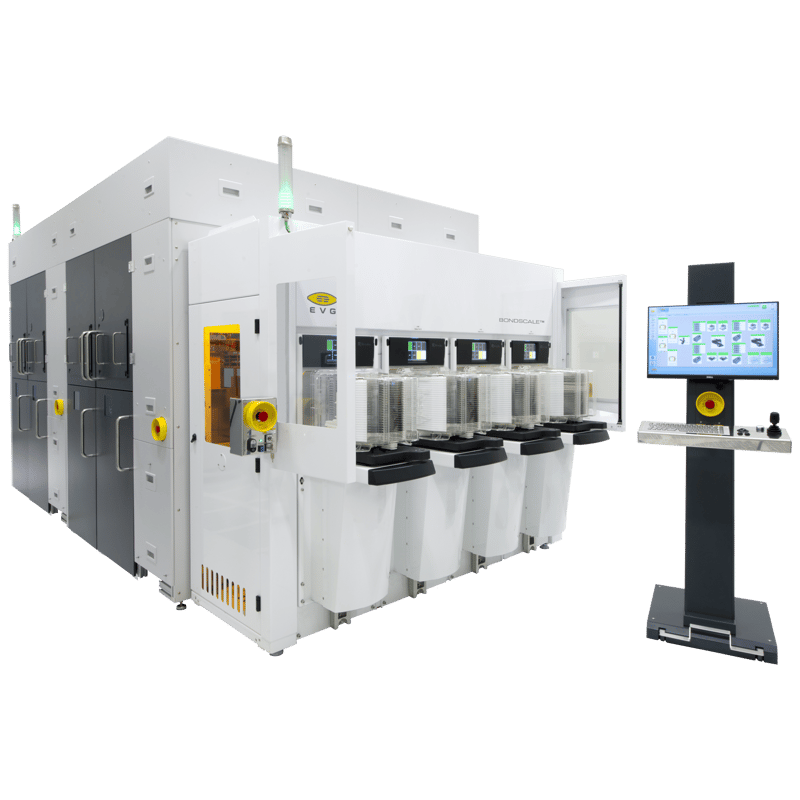
BONDSCALE
What is the EVG® BONDSCALE?
The EVG® BONDSCALE is designed to support a wide range of fusion and molecular wafer bonding applications, including engineered substrate manufacturing and 3D integration approaches such as monolithic 3D (M3D) layer-transfer processing. By bringing wafer bonding into front-end semiconductor processing, BONDSCALE addresses long-term challenges for "More Moore" logic device scaling, as outlined in the International Roadmap for Devices and Systems (IRDS).
IES is the official UK representative for EV Group (EVG), supplying, installing, and supporting BONDSCALE for customers across the UK.
What makes it more productive than existing fusion bonding platforms?
Incorporating advanced edge alignment technology, BONDSCALE boosts wafer bond productivity and reduces cost of ownership (CoO) compared to existing fusion bonding platforms.
How does it fit alongside EVG's GEMINI FB XT?
BONDSCALE is sold alongside EVG's GEMINI FB XT automated fusion bonding system, with each targeting different application needs: BONDSCALE is aimed at engineered substrate bonding and layer-transfer processing, while the GEMINI FB XT is optimised for applications that demand higher alignment accuracy, such as memory stacking, 3D systems on chip (SoC), backside illuminated CMOS image sensor stacking, and die partitioning.
Where can I buy or get support for BONDSCALE in the UK?
As EV Group's official UK representative, IES provides UK-based sales, installation, and engineering support for BONDSCALE and the wider EVG bonding equipment portfolio.
Features:
- Fully automated fusion/molecular wafer bonding applications on 200 mm and 300 mm substrates in a single platform
- Direct wafer bonding with plasma activation for heterogeneous integration of different materials, high-quality engineered substrates as well as thin-silicon layer-transfer applications
- Layer-transfer processes and engineered substrates enabling logic scaling, 3D integration such as M3, 3D VLSI including backside power distribution, N&P stacking, logic-on-memory, clustered functional stacks and beyond-CMOS adoption
Technical Data:
- Wafer diameter (substrate size) - 200, 300 mm
- Max. number or process modules - 8
- Throughput - Up to 40 Wafers per hour
- Handling system - 4 Loadports
- Features -
| Up to eight pre-processing modules like clean module, LowTemp™ plasma activation module, alignment verification module and debond module available |
| XT Frame concept for highest throughput with EFEM (Equipment Frontend Module) |
| Optical edge alignment module: Xmax/Ymax = 18 µm 3 σ |
Applications:
- Engineered Substrate Manufacturing
BONDSCALE facilitates the creation of high-quality engineered substrates, supporting the development of advanced semiconductor devices. - Layer-Transfer Processes
The system is adept at handling layer-transfer processes, enabling the integration of different materials and the development of complex semiconductor structures. - Monolithic 3D Integration (M3D)
BONDSCALE supports M3D integration, allowing for the stacking of multiple layers of semiconductor devices to enhance performance and reduce form factor. - Beyond-CMOS Applications
The system is also applicable in beyond-CMOS technologies, facilitating the adoption of new materials and architectures in semiconductor devices.