




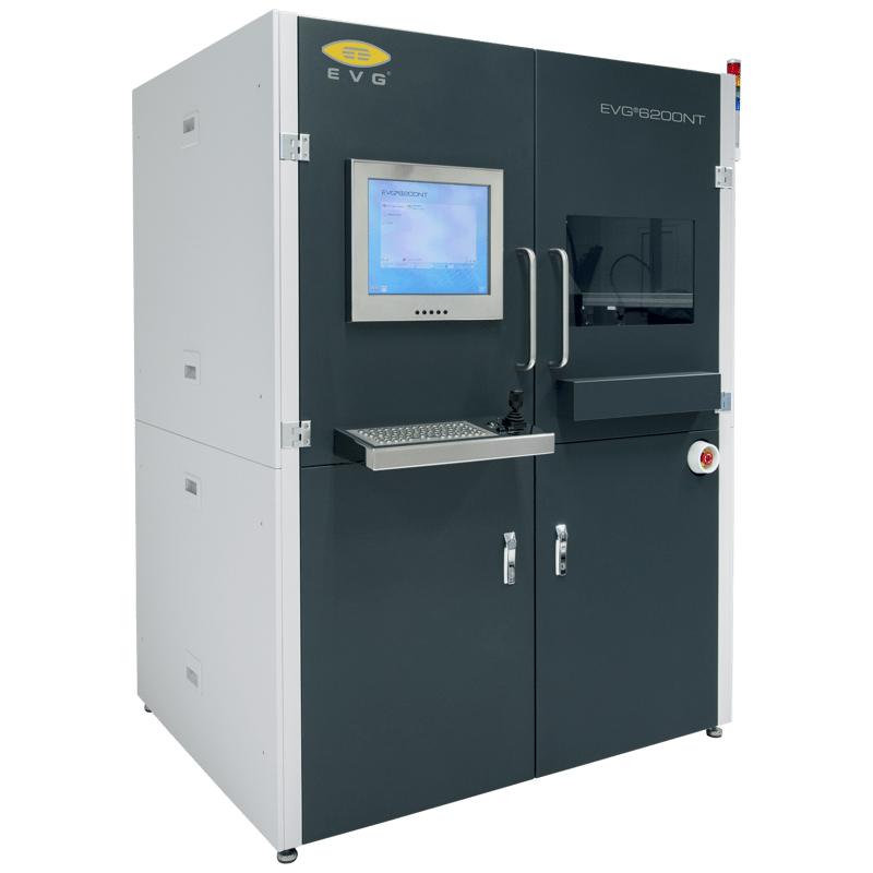
EVG®6200 NT
What is the EVG®6200 NT?
The EVG®6200 NT is a high-performance mask alignment system built for environments that need both flexibility and throughput, handling substrates from small pieces up to 200 mm wafers on a compact footprint. It's available in semi-automated and fully automated configurations, including the fully enclosed Gen 2 version, meeting the rigorous standards of high-volume manufacturing. IES is the official UK representative for EV Group (EVG), supplying, installing, and supporting the EVG®6200 NT for customers across the UK.
What alignment and process capabilities does it offer?
Integrated vibration isolation and advanced alignment accuracy support a wide range of applications, including exposure of thin and thick resists, deep cavity patterning, and processing of delicate materials such as compound semiconductors. The system also supports EV Group's proprietary SmartNIL™ nanoimprint lithography technology, alongside standard vacuum, hard, soft, and proximity exposure modes.
What makes it suitable for high-volume manufacturing?
Automated contact-free wedge compensation and a dynamic alignment function with real-time offset correction keep results consistent at scale, while the system's field upgrade path from semi-automated to fully automated configuration lets facilities scale up without replacing the platform. Its multi-user concept (unlimited user accounts and recipes, assignable access rights, multiple UI languages) supports shift-based production teams as well as R&D users.
What reduces downtime and cost of ownership?
Quick mask and tooling changes, intuitive operator-friendly software, manual substrate loading capability even on the automated system, and a robust global support network make the EVG®6200 NT a reliable solution for demanding production and research environments alike.
Where can I buy or get support for the EVG®6200 NT in the UK?
As EV Group's official UK representative, IES provides UK-based sales, installation, and engineering support for the EVG®6200 NT and the wider EVG mask, bond, and NIL alignment portfolio.
Features:
- Wafer/substrate size from pieces up to 200 mm/8’’
- System design supporting versatility of lithography processes
- Throughput up to 180 WPH in first print mode or up to 140 WPH in automatic alignment mode
- Fragile, thin or warped wafer handling of multiple wafer sizes with quick change-over time
- Automated contact-free wedge compensation sequence with proximity spacers Auto origin function for precise centering of alignment key
- Dynamic alignment function featuring real-time offset correction
- Supports the latest UV-LED technology
- Rework sorting wafer management and flexible cassette system
- Manual substrate loading capability on automated system
- Field upgradeable from semi-automated to fully automated version
- Minimized system footprint and facility requirements
- Multi-user concept (unlimited number of user accounts and recipes, assignable access rights, different user interface languages)
- Advanced Software features and compatibility between R&D and full-scale production
- Agile processing and conversion re-tooling
- Remote tech support & SECS/GEM compatibility
- Table top or stand-alone version with anti-vibration granite table
- Additional capabilities:
- Bond alignment
- IR alignment
- Nanoimprint lithography (NIL)
Applications:
- Mask-based photolithography (optical lithography)
Standard patterning of photoresist via mask exposure, with alignment, for microfabrication/metrology. - Double-sided / back-side lithography
Because it supports bottom-side and IR alignment, it’s well suited for processes where features are needed on both sides of a wafer (e.g. through‑wafer vias, MEMS membranes, backside contacts). - Nanoimprint lithography (NIL / SmartNIL®)
Using imprint (stamp) techniques to replicate nanoscale patterns, especially where high resolution and fidelity are needed. - Wafer/substrate bonding & alignment
Bond alignment (aligning two wafers or substrates before bonding) is supported; useful for stacked device architectures, 3D integration, heterogeneous integration. - Patterning challenging topographies / non-ideal substrates
Because the 6200 NT supports fragile, warped, bowed substrates, it can handle patterning on less-than-perfect surfaces (e.g. non‑flat materials, nonstandard wafers). - High-throughput R&D / pilot production
The throughput, automation, and industrial features make it suitable not just for lab-scale work, but transitional environments (pilot lines) or small-volume production. - Process transfer / bridging to production
Because its modes, automation, and handling features mirror those required for manufacturing, processes validated on the 6200 NT can be more easily transferred to full-scale production tools. - Advanced devices: MEMS, photonics, sensors, power devices
In domains requiring precise overlay, alignment, multi-layer stacking, or imprint-based nanoscale features, the 6200 NT can serve as both development and limited-run fabrication tool. - Metrology, overlay verification, alignment studies
Its alignment accuracy and dynamic alignment features make it useful in process development / research for validating alignment fidelity, overlay errors, or alignment strategies.