




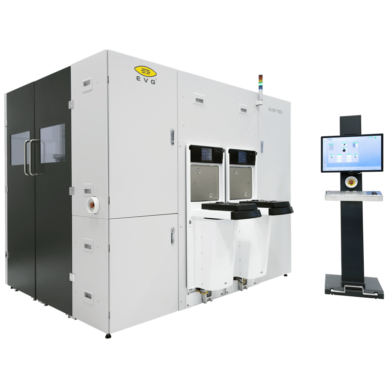
EVG®150
What is the EVG®150?
The EVG®150 is a fully modular, automated resist processing tool designed for high-throughput spin, spray, and develop processes. Its ultra-compact footprint of less than 3 m², combined with a redesigned modular structure, gives easy access to individual chambers and robot areas for streamlined operation and maintenance.
IES is the official UK representative for EV Group (EVG), supplying, installing, and supporting the EVG®150 for customers across the UK.
What throughput and processing capacity does it offer?
The system features four wet processing modules and up to 20 bake/chill units, delivering outstanding throughput for real-life production processes. A high-speed, high-accuracy robot with advanced scheduler algorithms maximises throughput while maintaining process quality. Despite its compact design, the EVG®150 can accommodate up to 12 pumps and resist bottles within the main frame, giving a highly flexible and scalable solution.
How does it handle high-topography wafers and specialist coatings?
The EVG®150 guarantees uniform coatings across a wide range of applications, from thick resists to sub-micron layers, and is well suited to wafers with high topography thanks to EVG's proprietary OmniSpray™ ultrasonic atomisation technology. With up to four XY spray coat modules, it delivers unrivalled spray coating throughput.
What applications is it used for?
The EVG®150 is used in MEMS, image sensors, advanced packaging, RF, 5G, 3D sensing, photonics, automotive, and power electronics manufacturing. See applications below.
Where can I buy or get support for the EVG®150 in the UK?
As EV Group's official UK representative, IES provides UK-based sales, installation, and engineering support for the EVG®150 and the wider EVG resist processing and lithography portfolio.
Features:
- Wafer sizes up to 300 mm Up to six process modules
- Customizable number - up to twenty bake/chill/vapor prime stacks
- Up to four FOUP load ports or cassette loading
- Available modules include Spin Coat, Spray Coat, NanoCoat™, Develop, Bake/Chill/Vapor/Prime
- EV Group’s proprietary OmniSpray® ultrasonic atomization technology provides unmatched process results when it comes to conformal coating of extreme topographies
- Optional NanoSpray™ module achieves conformal coating of 300-micron deep patterns with aspect ratios up to 1:10 and vertical sidewalls
- Extensive range of supported materials
- Bake modules for up to 250 °C
- Megasonic technology for cleaning, sono-chemical processing and developing improves process efficiency and lowers the process time from hours to minutes
- Sophisticated and field-proven robot handling with dual end-effector capability ensures continuous high throughput
- Handling of thick or ultra-thin, fragile, bowed or small-diameter wafers
- Versatile combinations of multi-functional modules for spin and spray coating, developing, bake and chill provide great opportunities in many fields of application EFEM (Equipment Frontend Module) and optional FSS (FOUP Storage System)
- Process technology excellence and development service
- Multi-user concept (unlimited number of user accounts and recipes, assignable access rights, different user interface languages)
- Smart process control and data analysis feature [Framework SW Platform]
- Integrated analysis features for process and machine control
- Equipment and process performance tracking feature
- Parallel/queueing task processing feature
- Smart handling features
- Occurrence and alarm analysis
- Smart maintenance management and tracking
Applications:
- MEMS / microsystems
Many MEMS devices have complex topography (trenches, cavities). The spray / OmniSpray capabilities help coat these uniformly. - Image sensors / photonics
High-uniformity resist coating & development is critical for pattern fidelity, overlay, optical elements, etc. - Advanced packaging / 3D integration
In packaging, resist layers may be applied over non-flat surfaces, bumps, vias — the modular and coating features help. - RF / 5G / high-frequency devices
Devices with varying topography, mixed materials, and stringent process control benefit from the versatility. - Power electronics / automotive
These often use larger features, possibly thick resist layers, robust patterning, sometimes uneven substrates. - General semiconductor back-end / lithography flows
Any process needing reliable, repeatable, high-throughput resist coating & development can use EVG 150. - High-topography / non-planar devices
Where classical spin coating fails (due to height variations), spray or ultrasonic coating helps. - R&D → production bridging
Because it’s modular and configurable, it’s suited both for research / development (trying new resists, flow changes) and small-volume production. - Multi‑project / mixed substrate processing
Its flexibility, modularity, and support for varying substrate shapes / sizes make it useful in multi-user / multi-discipline facilities.