




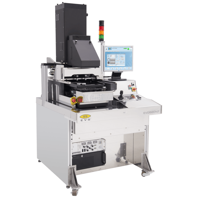
EVG®620 NT
What is the EVG®620 NT?
The EVG®620 NT is a mask alignment system built for optical double-side lithography, scaling from R&D use up to high-volume production. It's available in semi-automated or fully automated configurations — including a fully housed Gen 2 version — to meet fab standards and high-volume requirements. IES is the official UK representative for EV Group (EVG), supplying, installing, and supporting the EVG®620 NT for customers across the UK.
What substrate sizes and processes does it support?
The EVG®620 NT handles substrates from small pieces up to 150 mm wafers (200 mm on the EVG®6200 NT variant), with fragile, thin, or warped wafer handling and quick change-over between wafer sizes. It supports standard lithography processes — vacuum, soft, hard, and proximity exposure modes — alongside EV Group's proprietary SmartNIL™ nanoimprint technology, capable of patterning features below 40 nm.
What makes it suitable for both R&D and production?
Integrated vibration isolation, automated contact-free wedge compensation, and a dynamic alignment function with real-time offset correction deliver consistent exposure results across thin and thick resists, deep cavities and complex topographies, and fragile materials such as compound semiconductors. The system is field-upgradeable from semi-automated to fully automated configuration, and its multi-user concept (unlimited user accounts and recipes, assignable access rights, multiple UI languages) supports both single-operator R&D labs and shift-based production teams.
What reduces downtime and cost of ownership?
Operator-friendly software, minimised time for mask and tooling changes, manual substrate loading capability even on automated systems, and worldwide service and support keep the EVG®620 NT running efficiently in any manufacturing environment.
Where can I buy or get support for the EVG®620 NT in the UK?
As EV Group's official UK representative, IES provides UK-based sales, installation, and engineering support for the EVG®620 NT and the wider EVG mask, bond, and NIL alignment portfolio.
Features:
- Wafer/substrate size from pieces up to 150 mm/6’’
- System design supporting versatility of lithography processes
- Fragile, thin or warped wafer handling of multiple wafer sizes with quick change-over time
- Automated contact-free wedge compensation sequence with proximity spacers
- Auto origin function for precise centering of alignment key
- Dynamic alignment function featuring real-time offset correction
- Supports the latest UV-LED technology
- Rework sorting wafer management & flexible cassette system
- Manual substrate loading capability on automated system
- Field upgradeable from semi-automated to fully automated version
- Minimized system footprint and facility requirements
- Multi-user concept (unlimited number of user accounts and recipes, assignable access rights, different user interface languages)
- Advanced SW features and compatibility between R&D and full-scale production
- Agile processing and conversion re-tooling
- Remote tech support and SECS/GEM compatibility
- Additional capabilities:
- Bond alignment
- IR alignment
- Nanoimprint lithography (NIL)
Applications:
Optical Photolithography / Mask-based Patterning
Standard UV-based resist patterning via mask exposure and alignment, in research or small-volume production.
Double‑Sided / Backside Lithography
Because it supports bottom-side alignment and IR alignment, users can pattern features on both faces of a wafer or substrate (e.g. for through-wafer vias, MEMS structures)
Nanoimprint Lithography (UV‑NIL / SmartNIL®)
The tool supports imprint-based replication of nanoscale patterns using stamps/molds, enabling high-resolution features (≤ ~40 nm) depending on the resist, imprint mold, and process.
Bond Alignment / Wafer-to-Wafer Alignment
It can align wafers or substrates before bonding (e.g. for stacking, 3D integration) using bond alignment modes.
Patterning Challenging Substrates / Topographies
Because of its precise alignment, wedge compensation, and capability to handle warped/fragile substrates, it’s suited for patterning on non-ideal surfaces, deep cavities, thick or thin resist films, and for materials like compound semiconductors.
R&D / Pilot Production / Tool Development
Its flexibility (semi-automated & upgrade path to full automation) makes it useful in research labs, pilot lines, and technology development environments.
Migration to Volume Manufacturing
Processes developed on the 620 NT (especially using SmartNIL / aligned imprint) can feed into larger-scale production tools, due to mode compatibility and automation support.
Micro- / Nano-Electronics, MEMS, Photonics, Sensors
In device domains requiring precise patterning, alignment, multi-layer stacking, or nanoscale structure replication, the 620 NT serves as a testbed or development platform.
Metrology & Process Validation
Because of its alignment precision and stability, it may also be used to validate mask/wafer overlay, alignment accuracy, and lithographic fidelity in process development studies.