




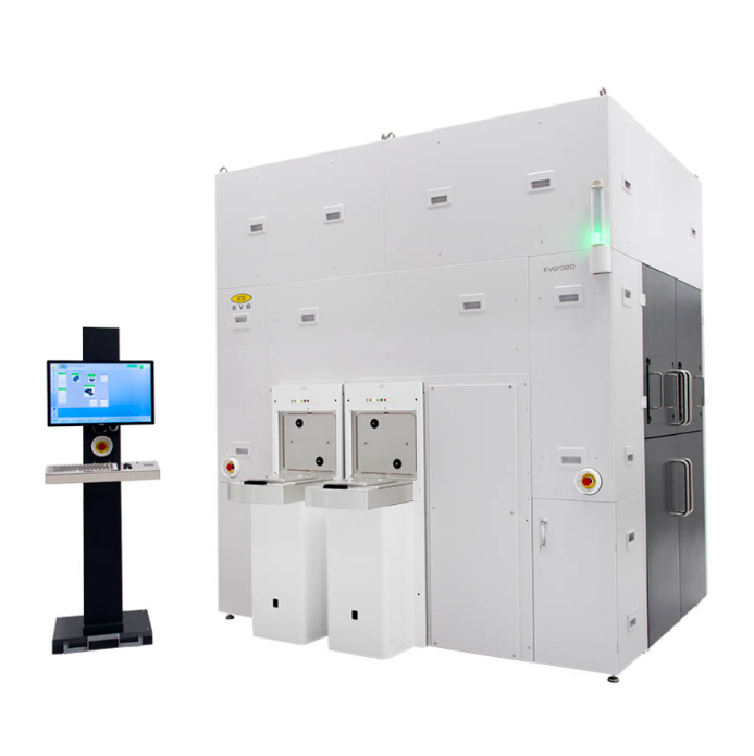
EVG®320
What is the EVG®320?
The EVG®320 is an automated single wafer cleaning system that handles wafers and substrates automatically between process stations. IES is the official UK representative for EV Group (EVG), supplying, installing, and supporting the EVG®320 for customers across the UK.
How does the EVG®320 handle wafer loading and alignment?
Equipped with a robotic handling system, the EVG®320 ensures precise pre-alignment and loading of wafers, removing the need for manual handling between process stations.
What operating modes does the EVG®320 support?
The EVG®320 supports both cassette-to-cassette and FOUP-to-FOUP operations, making it adaptable to different fab material-handling formats.
Where can I buy or get support for the EVG®320 in the UK?
As EV Group's official UK representative, IES provides UK-based sales, installation, and engineering support for the EVG®320 and the wider EVG wafer cleaning portfolio.
Features:
- Up to four cleaning stations
- Fully automated cassette-to-cassette or FOUP-to-FOUP handling
- Edge handling for double-sided cleaning processes available (option)
- High-efficiency cleaning using 1 MHz megasonic nozzles or area transducers (option)
- Advanced remote diagnostics
- Prevents cross-contamination from back to front side
- Fully software controlled cleaning process
Technical Data:
Wafer diameter (substrate size) - 200, 100 - 300 mm
Cleaning system
- Open chamber, spinner and cleaning arm
- Chamber: made of PP or PFA (option)
- Cleaning media: DI-water (standard), other cleaning media (option)
- Spinner chuck: vacuum chuck (standard) and edge handling chuck (option) made of metal ion free and clean materials
- Rotation: up to 3000 rpm (in 5 sec)
Megasonic nozzle
- Frequency: 1 MHz (3 MHz option)
- Output power: 30 - 60 W
- DI-water flow rate: up to 1.5 liter/min
- Effective cleaning area: Ø 4.0 mm
- Material: PTFE
Applications:
- Pre-Bonding Cleaning: Essential for preparing wafers before bonding processes such as fusion or hybrid bonding, ensuring surfaces are free from contaminants.
- Post-Debonding Cleaning: Used to remove residual bonding materials after debonding processes, preparing wafers for reuse or further processing.
- Advanced Packaging and 3D Integration: Supports applications requiring high cleanliness standards, such as 3D system-on-chip (SoC) devices and advanced packaging solutions.
- MEMS and Semiconductor Device Fabrication: Plays a crucial role in the fabrication of microelectromechanical systems (MEMS) and semiconductor devices, where surface cleanliness is critical for device performance and reliability.