




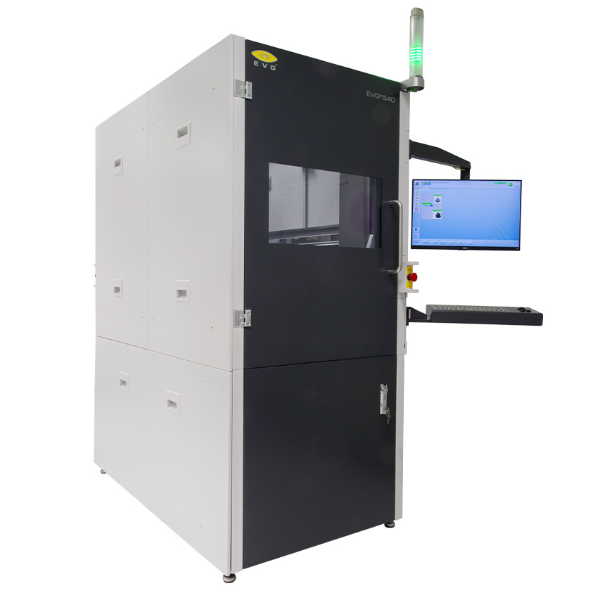
EVG®540
What is the EVG®540?
The EVG®540 is an automated single-chamber production bonder designed for pilot-line manufacturing and R&D in wafer-level packaging, 3D interconnect, and MEMS applications. IES is the official UK representative for EV Group (EVG), supplying, installing, and supporting the EVG®540 for customers across the UK.
What applications is the EVG®540 used for?
The EVG®540 is used for:
Wafer-level packaging
3D interconnect
MEMS applications
How does the EVG®540 support the move from R&D to production?
Built on a modular design, the EVG®540 offers a proven solution for seamlessly transitioning wafer bonding processes from R&D to large-scale manufacturing. It integrates smoothly with EVG's fully integrated production bonding systems, so processes developed on the EVG®540 carry through to higher-volume manufacturing without redevelopment.
Who is the EVG®540 designed for?
It's built for pilot-line manufacturing and R&D teams working on wafer-level packaging, 3D interconnect, and MEMS, who need an automated, production-representative bonder before scaling to full-volume manufacturing.
Where can I buy or get support for the EVG®540 in the UK?
As EV Group's official UK representative, IES provides UK-based sales, installation, and engineering support for the EVG®540 and the wider EVG wafer bonding portfolio.
Features:
- Single-chamber bonder up to 300 mm substrate size
- Compatible with SmartView® and MBA300
- Automatic handling of up to four bond chucks
- Compliant to high safety standards
Technical Data:
- Maximum Heater size - 300 mm
- Loading chamber - 2 axis robot
- Max. bond chambers - 1
Applications:
- Wafer-Level Packaging & 3D Interconnects
As devices move toward 3D stacking, interposer integration, and heterogeneous integration, the ability to bond large wafers with alignment and consistency is crucial. The 540 serves as a production-capable tool in such flows. - MEMS & Sensor Packaging
MEMS devices often require hermetic sealing or wafer capping, and bonding is key to packaging them. The 540 can support these in higher throughput compared to lab-scale bonders. - Technology Transfer / Scale-Up
Processes developed on smaller or semi-automated bonders (like EVG 501, 510, 520) can be ported to the 540 more directly, because of its more “production-like” automation and throughput. - Pilot Manufacturing / Pre-Production Runs
For small-volume devices or new product lines, the 540 provides a balance of automation, capacity, and flexibility. - Integration with Alignment & Pre‑Processing Tools
Because it’s compatible with EVG’s alignment (SmartView) and handling modules (MBA300), it can be part of an integrated wafer processing / bonding line.