




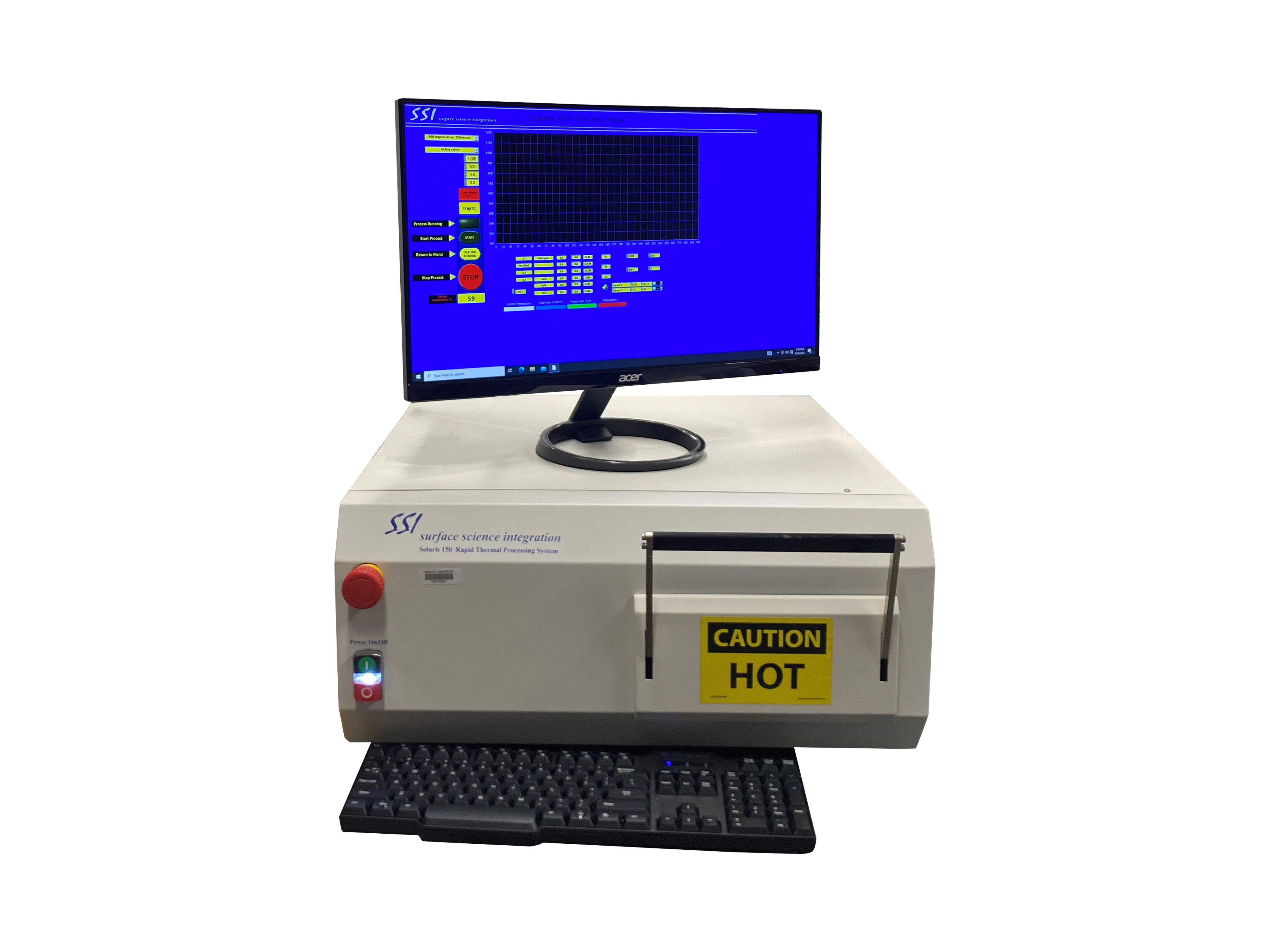
Solaris 200
What is the Solaris 200 RTP system?
Rapid thermal annealing furnaces offer a wide range of applications such as annealing for silicon and compound semiconductor wafers (RTA), rapid thermal oxidation (RTO), rapid thermal nitriding (RTN), rapid thermal diffusion from a spin-on dopant, crystallisation, and contact alloying. The Solaris 200 is a compact, manually loaded RTP system engineered for research and development applications, supporting substrates up to 200 mm.
IES is an equipment partner for SSI (Surface Science Integration), supplying, installing, and supporting the Solaris 200 for customers across the UK.
How does it achieve consistent, repeatable results?
The Solaris uses a unique PID process controller that ensures accurate temperature stability and uniformity. It's designed for silicon implant annealing and monitoring, as well as compound semiconductor implant activation and ohmic alloying.
What gas handling capability does it offer?
The system can accommodate six interlocked mass flow controllers (MFCs) for gas mixing and forming gas processing — a step up from the four-MFC configuration on the smaller Solaris 150mm, giving greater flexibility for multi-gas process recipes.
Can the system be customised?
This system has state-of-the-art options available and is customisable by the end user on purchase. IES works with buyers on every additional feature needed to deliver a final product that meets the laboratory demands of the modern scientist. Customers interested in these customisable options are encouraged to contact a sales representative in their area.
Where can I buy or get support for the Solaris 200 in the UK?
As an equipment partner for SSI, IES provides UK-based sales, installation, and engineering support for the Solaris 200 and the wider SSI rapid thermal processing portfolio, including the Solaris 150mm.
Main Features
-
Wafer handling: Manual loading of wafer into the oven, single wafer processing
-
Wafer sizes: 2", 3", 4",5",6",8"
-
Ramp up rate: 1-150°C per second, user-controllable.
-
Recommended steady state duration: Unlimited, dependent on Temp & cooling
-
Ramp down rate: Temperature Dependent, max 150°C per second.
-
Recommended steady state temperature range: RT - 1200°C
-
Temperature accuracy: +1.78°C total errors
-
Thermocouple temperature accuracy: +1.1°C
-
Temperature repeatability: +2°C or better at Steady State
-
For a titanium silicidation process, no more than 4% increase in non-uniformity during the first anneal at 650°C to 700°C.
Technologies
The Solaris RTP system is a versatile tool that is useful for many applications:
-
Ion Implant Activation
-
Polysilicon Annealing
-
Oxide Reflow
-
Silicide Formation
-
Contact Alloying
-
Oxidation and Nitridation
-
GaAs Processing
Applications
- Semiconductor fabrication: Devices on 200 mm wafers (or smaller), including logic, MEMS, power devices, sensors.
- Compound semiconductor / III‑V device manufacturing: GaAs, InP, GaN, etc. The tool supports compound substrate processing.
- MEMS / microsystems: Small sensors/devices often need precision thermal treatment and may operate on non‑standard substrates.
- Advanced research labs / university clean‑rooms: For prototyping new materials, new device architectures, small volumes.
- Specialty electronics (e.g., aerospace, medical, defence): Where low volume but high reliability is essential, and custom thermal profiles are needed.