




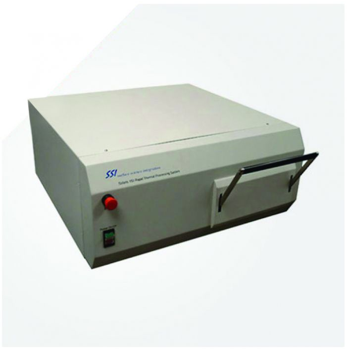
Solaris 150
What is the Solaris 150mm RTP system?
The Solaris 150mm is a manual loading, benchtop rapid thermal processing (RTP) system from Surface Science Integration (SSI), engineered for a wide range of semiconductor applications, including silicon and compound wafer annealing (RTA), rapid thermal oxidation (RTO), nitridation (RTN), and diffusion using spin-on dopants. It processes substrates up to 150 mm (152.4 mm) in diameter, as well as smaller wafers and pieces (2", 3", 4", and 5"), for R&D and pre-production use.
IES is an equipment partner for SSI, supplying, installing, and supporting the Solaris 150mm for customers across the UK.
What additional capabilities does it offer?
Additional capabilities include crystallisation, contact alloying, and advanced phase modification to optimise material properties, interfaces, and stress profiles. The Solaris is designed for silicon implant annealing and monitoring, as well as compound semiconductor implant activation and ohmic alloying.
How does it achieve precise temperature control?
The system's unique temperature measurement approach requires virtually no calibration for different wafer types and backside emissivity differences, and a PID process controller ensures accurate temperature stability and uniformity across the RT–1300°C processing range.
What throughput and process flexibility does it offer?
Originally developed for ion implant anneal, RTP technology has evolved to support processes such as oxidation, silicide formation, and selected CVD steps. Offering fast ramp rates (typically 20–150°C/sec) and precise control across processing temperatures from ~200°C to 1300°C, the Solaris 150mm enables high-throughput, multistage thermal cycles in a controlled gas environment — all within a single recipe. The system can accommodate four interlocked mass flow controllers (MFCs) for gas mixing and forming gas processing.
Where can I buy or get support for the Solaris 150mm in the UK?
As an equipment partner for SSI, IES provides UK-based sales, installation, and engineering support for the Solaris 150mm and the wider SSI rapid thermal processing portfolio.
Features
- Sample sizes up to 6inch in diameter
- Small foot print
- Uniform heating, with lamps top and bottom of the sample
- Stable and repeatable temperature control
- Temperature range up to 1200°C
- Zone temperature control for enhanced process control
- High purity quartz wafer holder and chamber
- Gold reflectors for fast heating rate
- Up to 6 mass flow controllers
- Quartz liner available for BPSG/PSG processing
- SIC coated graphite susceptor is available for compound semiconductor samples
Technologies
- Ion Implant Activation
- Polysilicon Annealing
- BPSG/PSG Reflow
- Silicide Formation
- Ti/Au Nanotube Ohmic Contact Formation
- Contact Alloying
- Oxidation and Nitridation
- GaAs and III-V Ohmic Alloying
Applications
- Semiconductor / micro‑electronics: Classic fit — wafer processing, device fabrication, implant activation, contact alloying, silicide formation.
- MEMS / sensor manufacturing: Devices built on wafers or small substrates that need thermal treatment, especially small batch or specialist sensors.
- Compound semiconductors / III‑V devices: Some sources list GaAs, III‑V alloying/ohmic contact applications.
- Advanced materials / research institutions: Universities, clean‐rooms, labs that require rapid thermal processing capabilities on smaller wafer sizes.
- Prototype / startup fabs: Where throughput is lower but flexibility and small footprint are important.