


Semiconductor Equipment and Process Training from IES
IES offers a variety of courses that cover a wide range of topics central to the semiconductor industry.
3 min read
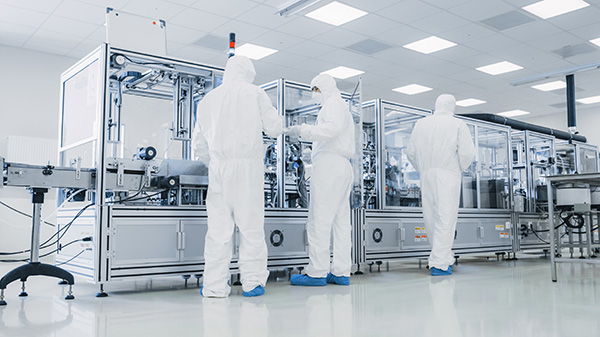
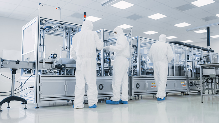
Semiconductor manufacturing involves hundreds of process steps, dozens of interdependent tools, and tolerances measured in nanometres.
At that level of precision, equipment performance isn't just important, it's everything. When a tool goes down or drifts out of spec, production delays and costs mount fast.
That's why field service engineers (FSEs) are so critical. But FSE support isn't one-size-fits-all.
The skills, knowledge, and activities required vary significantly depending on which part of the process you're supporting, whether it's diffusion, photolithography, etch, thin film, backend or metrology.
Here's a complete breakdown of the six core areas of semiconductor manufacturing, and the types of activities you may need FSE support with for each one.
Diffusion is the starting point of semiconductor device manufacturing.
Vertical and horizontal furnaces grow layers of oxide, nitride, or polysilicon onto silicon wafers at around 1,100°C, processing up to 200 wafers at a time using oxygen, hydrogen, and steam. Get this foundational step wrong, and the impact ripples through everything that follows.
FSEs supporting diffusion furnaces need to be comfortable working with high-temperature systems and precise gas control. Key activities include:
Find out how we support diffusion equipment here.

Photolithography is the process of transferring circuit patterns onto a wafer surface using light. Each new layer must align precisely with the one beneath it. Get the alignment wrong, and the device won't function.
Karl Suss, ASML, Nikon, Ultratech, Canon and EVG are among the most widely used tools in this area.
FSEs working in photolithography need a strong understanding of optical systems and wafer handling mechanics. The most common support activities are:
photolithography tools are also sensitive to environmental conditions. FSEs often need to look beyond the tool itself and consider vibration, temperature, and cleanliness in the surrounding environment.
Find out how we support photolithography equipment here.
Once a pattern has been exposed, etch removes the unwanted material.
Dry etch dominates in modern fabs, with Reactive Ion Etching (RIE), Deep Reactive Ion Etching (DRIE), and plasma etch being the main techniques. Tools from KLA, SPTS, Oxford Instruments, and Applied Materials are common in this area.
Wet clean and etch also play an important role, with manual, semi-automated, and fully automated equipment from AMAT, LAM, and EBARA widely used across fabs.
Etch processes are highly sensitive to chamber conditions. Small deviations in vacuum, gas flow, or plasma uniformity can result in under-etching, over-etching, or uneven results, any of which can render a wafer unusable.
FSE support here focuses on:
Find out how we support etch equipment here.

Thin-film deposition adds ultra-thin layers of materials (including metals, dielectrics, and semiconductors) to the wafer surface. These layers form the conductive pathways and insulating barriers that make the device function.
Physical Vapour Deposition (PVD) and Chemical Vapour Deposition (CVD) are the dominant deposition methods, with thin-film tools from KLA, SPTS, Applied Materials, and Veeco widely used.
Film quality (thickness, composition, uniformity) is critical, and maintaining the tools that produce it requires real hands-on technical skill.
FSE activities in thin film include:
Find out how we support thin-film equipment here.

Backend takes the completed wafer and turns it into a usable, shippable chip through dicing, die attach, wire bonding, and encapsulation.
It's also where Chemical Mechanical Planarisation (CMP) increasingly comes into play. As chip designs become more complex and require higher levels of metallisation interconnects, CMP is needed more frequently to flatten each layer before the next one is added.
Tools commonly supported include AMAT Mirra/MESA, MIRRA/Ontrak, and AXUS.
FSE support in backend spans:
Find out how we support backend equipment here.

Metrology is the measurement and inspection layer that tells you whether each step has been performed within specification. Without reliable metrology, every other process is flying blind.
Because metrology tools are used to verify the accuracy of everything else, their own accuracy is non-negotiable.
Common equipment includes detection, measurement and microscope tools, while FSE activities include:
Find out how we support metrology equipment here.

Need on-site semiconductor support? View IES's Field Service Engineer capabilities:

IES offers a variety of courses that cover a wide range of topics central to the semiconductor industry.
Factory de-installations are never simple. But they’re a lot easier when you do them right.
Supporting implant equipment in fabs and cleanroom environments requires a unique combination of technical expertise, problem-solving skills and an...