


Q240
The Q 240 is the largest member of the Q-series—optimized for handling multiple wafers up to 200 mm in diameter. Designed with a quartz glass process chamber, it’s built to accommodate high-throughput plasma processing in demanding industrial and research environments.
Key Features:
High-Capacity Processing
- Processes up to 50 wafers (≤ 200 mm diameter) simultaneously—perfect for research, prototyping, or small-scale production.
Robust Process Chamber
- A quartz glass cylinder with a 240 mm inner diameter and 450 mm internal depth, providing a generous 20-liter volume.
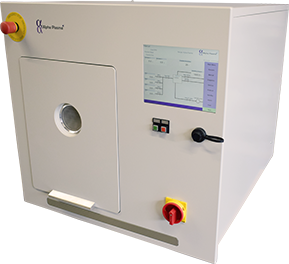
Compact Footprint & Solid Build
- Dimensions: 760 mm (L) × 775 mm (W) × 775 mm (H), weighing 100 kg—ideal for cleanroom table or wall installation.
Advanced Microwave Power
- Operates at 2.45 GHz, with adjustable power output ranging from 50 W to 1,200 W, enabling flexible control over plasma density and energy.
Flexible Gas Handling
- Includes one internal gas channel by default, expandable to three channels for multi-gas process recipes.
Optional Substrate Support
- Features a customizable aluminum wafer holder tailored to your specific workflow and wafer layout needs.
Vacuum & Venting Infrastructure
- Equipped with a DN 40 ISO-KF vacuum connection and electromagnetic solenoid valve venting for precise atmosphere control.
Technical Data:
- Dimensions: L: 760mm W: 775mm H: 775mm
- Weight: 100 KG
- Volume: 20 Liter
- Process chamber: quartz glass, 240mm Ø, B: 450mm
- Microwave output: 2,45 GHz / 50 - 1200 Watt
- Inclusive: 1 gas channel (gas distribution system inside the process chamber), up to 3 channels available
- Substrate holder (optional): aluminium, custom design possible
- Vacuum connection: DN 40 ISO-KF
- Venting: electromagnetic solenoid valve
- Pump system: up to 40m³/h
- Chamber door: you can choose between hinged-type with viewing port and drawer door with attached support rods
- Wafer size: up to 200mm, at a number of 50 wafers
Applications:
- Semiconductor / MEMS manufacturing: Wafer sizes up to 200 mm and the process steps (resist removal, etching) make it a natural fit.
- Micro-electronics / sensor modules: Where wafers or substrate circular formats up to ~200 mm are used.
- R&D / pilot lines: For labs working on device prototypes, needing a compact but high-quality plasma system.
- Clean-room component manufacturing: For example, in packaging, post‐implant cleaning, or surface prep of wafers or devices.
- Advanced materials / surface science: Where high-purity plasma systems are required to treat surfaces or thin‐films before coating or bonding.