


AL18 M
The Alpha Plasma System AL 18 is a compact, high-performance plasma processing solution that brings flexibility, precision, and robust engineering to semiconductor packaging and R&D environments. Its modular design, advanced microwave plasma capabilities, and optional enhancements offer customers a tailored toolset to streamline production and achieve uniform results across multiple packaging tasks.
Key Features:
- Cutting-Edge Plasma Technology: Incorporates Alpha Plasma’s proprietary design with microwave coupling, enabling multiple operational modes—including the proven Electron Cyclotron Resonance (ECR)—for exceptional process flexibility.
- Rotary Table Option: Supports classic rotary table configurations for enhanced sample throughput and ease of loading
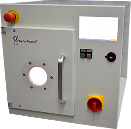
Technical Data:
- Process chamber: Aluminum
- Volume: 18 liters
- Chamber size: W 250 mm × D 290 mm × H 250 mm
- Chamber door: Hinged – type with viewing port
- Microwave power: 2.45 GHz, adjustable between 50 and 600 Watts
- Options:
- Vacuum pump
- Gas Channel
- Rotary table
- ECR set-up
- Utilities: 3/N/PE AC 50 Hz 400/240 V 16 A
- Dimensions: W 530 mm × D 600 mm × H 550 mm
- Weight: 40 kg w/o pump ; approx . 100 kg w/ vacuum pump
Applications:
- Semiconductors & Microelectronics Wafer cleaning, resist removal, surface activation before bonding or metallisation.
- MEMS & Sensors Preparation of surfaces before bonding, cleaning delicate microstructures, improving adhesion of sacrificial and functional layers.
- Advanced Packaging Surface activation prior to wire bonding, flip-chip attach, and encapsulation.
- Photonics & Optoelectronics Cleaning and activation of optical substrates prior to coating or assembly.
- Medical & Biomedical Devices Surface modification and activation for polymer bonding, biocompatible coatings, and implantable device preparation.
- Research & Development Material surface studies, functionalisation, plasma cleaning, and prototype fabrication.