


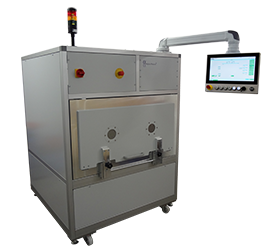
AL140
The Alpha Plasma System AL 140 is a high-capacity, industrial-grade microwave plasma system designed to handle large-scale flat substrates with outstanding efficiency. It’s ideally suited for applications in flat panel display, PCB manufacturing, and solar technology, catering to both production environments and research & development laboratories.
Key Features:
Large-Format Processing
- Perfectly engineered for treating wide or large substrates—making it an ideal solution for industries dealing with flat-panel displays, printed circuit boards, and solar cells.
Alpha Plasma
Versatile Surface Treatment
- Supports both plasma cleaning and plasma polymerisation, allowing transformation of surface properties—switching from hydrophobic to hydrophilic states (and vice versa)—and significantly enhancing adhesion for bonding, welding, and coating processes.
Material Neutrality
- There are no material limitations—this system works effectively across a wide range of substrates, providing great flexibility for production and R&D demands.
Technical Data:
- Plasma Source: Microwave 2.45GHz
- Microwave Power: Dual-Source, 2*1200W
- Chamber Size: W 850 x D 460 x H 350 mm
- Chamber Volume: 140L
- Process Gas: 3 standard process gas with MFCs
- Chamber Door: Drawer type with UV shield viewing port
- Operating System: 10.4” touch panel, Window CE based OS
Options:
- Vacuum System
- Green/ Red/ Yellow Light Tower
- Additional Gas Channel
Applications:
- Semiconductor / microelectronics The AL series is explicitly described as being used in semiconductor manufacturing. Clean, activated surfaces, vacuum processing, wafer-handling, etc are all relevant.
- Electronics & printed circuit boards (PCBs) Components such as sensors, PCBs, connectors often require cleaning, etching, adhesion improvement, or conformal coating after plasma treatment. The parylene technology application list includes electronics & sensors.
- Solar / photovoltaics The description mentions solar industry explicitly for the AL series.
- Plasma Parylene Systems For example, cleaning and surface activation of solar cell components or modules perhaps.
- Plastics / polymer substrates The AL system is also noted for plastics industry. Plasma activation can help adhesion of coatings on plastics or treat plastic parts.
- Automotive / harsh-environment electronics The parylene coatings list mentions automotive lighting systems, sensors in harsh environments, corrosion protection. Thus, the pretreatment plasma system (AL series) for such components makes sense.
- Aerospace / defence / medical (indirectly) Although the AL series is plasma, the downstream coating tech (parylene) is used in aerospace, medical devices etc, which implies that the pretreatment equipment also has relevance in these high-end industries.