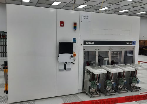
EVG®120
The EVG®120 is a fully automated, versatile resist processing tool designed to handle multiple substrate shapes and sizes up to 200 mm (8"). Its ultra-compact design, coupled with a dedicated chemistry cabinet for efficient chemical storage, enhances throughput and supports high-volume production environments. Optimised for the most demanding customer requirements, the EVG®120 delivers exceptional quality across a wide range of applications. With its focus on minimising total cost of ownership, this system ensures a cost-effective solution without compromising on performance or reliability.
Key Features:
- Wafer sizes up to 200 mm
- Ultra-compact design for minimal footprint
- Up to 2 coat/develop chambers and 10 hot/chill plates
- Versatile combinations of multi-functional modules for spin and spray coating, developing, bake and chill provide great opportunities in many fields of application
- Chemistry cabinet for external storage of chemicals
- EV Group’s proprietary OmniSpray® ultrasonic atomization technology provides unmatched process results when it comes to conformal coating of extreme topographies
- CoverSpinTM rotating cover for low resist consumption and optimized resist coating uniformity
- Megasonic technology for cleaning, sono-chemical processing and developing improves process efficiency and lowers the process time from hours to minutes
- Sophisticated and field-proven robot handling with dual end-effector capability ensures continuous high throughput
- Process technology excellence and development service
- Multi-user concept (unlimited number of user accounts and recipes, assignable access rights, different user interface languages)
- Smart process control and data analysis feature [Framework SW Platform] Integrated analysis features for process and machine control
- Equipment and process performance tracking feature
- Parallel/queueing task processing feature
- Smart handling features
- Occurrence and alarm analysis
- Smart maintenance management and tracking
Applications:
-
Advanced Packaging / Bumping / Dielectrics The EVG120 supports thick‐film resist coatings and spray processes that meet packaging demands (e.g., bumping, edge protection) per earlier product introductions. Handles non-standard wafer shapes, square substrates, odd geometries—all relevant in advanced packaging.
-
Compound Semiconductors / Photonics / “More than Moore” EVG states its resist-processing technology covers wide markets: advanced packaging, MEMS, MOEMS, sensors, microfluidics, RF devices, photonics. The press release for EVG120 specifically mentions order from VTT Technical Research Centre of Finland for “More than Moore” tech: MEMS, optoelectronics, photonics, compound semiconductors.
-
High-Topology / Irregular Substrates / Thick Resists The tool’s OmniSpray® and other features allow conformal coating on extreme topographies (e.g., high-aspect‐ratio cavities, warped wafers). It supports high viscosity resists (up to 52,000 cP) and thick coatings/resists.
-
R&D and Pilot Production Environments Because of its compact footprint and flexibility, the EVG120 is well suited for development labs, pilot production, multi‐project environments requiring diverse substrate sizes/shapes and frequent changeovers.
-
MEMS (Microelectromechanical Systems) The tool supports high‐topography coating (spray/OmniSpray) required in MEMS where device surfaces are not flat. Useful for devices such as sensors, actuators, microfluidic components that require patterned resists on non‐standard substrates.
Book a Live or Virtual Demo
See the capabilities of our partners' equipment - including EVG, scia Systems, Veeco, PPS and SSI - in action. Experience tailored demonstrations designed around your process and application needs.


