




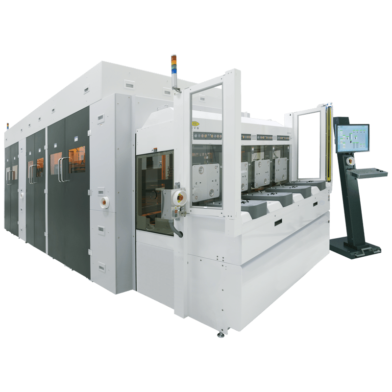
GEMINI
What is the GEMINI®?
The GEMINI® is a state-of-the-art, fully automated production wafer bonding system, combining wafer-to-wafer alignment and bonding processes in a modular design. IES is the official UK representative for EV Group (EVG), supplying, installing, and supporting the GEMINI® for customers across the UK.
What is the GEMINI® used for?
The GEMINI® is ideal for next-generation MEMS (Micro-Electro-Mechanical Systems) manufacturing up to 300 mm, excelling in wafer-level vacuum or overpressure encapsulation, as well as advanced system integration.
Why is the GEMINI® considered the industry standard for high-volume manufacturing?
The GEMINI® is the global industry standard for high-volume manufacturing (HVM). The platform includes up to four bond chambers, ensuring outstanding bond quality and high yield at production scale.
What bonding techniques does the GEMINI® support?
With full process flexibility, the GEMINI® supports a wide range of bonding techniques, including:
Metal bonding
Anodic bonding
Glass-frit bonding
Fusion bonding
Adhesive bonding
Where can I buy or get support for the GEMINI® in the UK?
As EV Group's official UK representative, IES provides UK-based sales, installation, and engineering support for the GEMINI® and the wider EVG wafer bonding portfolio.
Features:
- Fully automated and integrated platform for wafer-to-wafer alignment and wafer bonding
- Configuration options for bottom-side, IR or SmartView alignment
- Multiple bonding chambers
- Wafer handling system is separated from bond chuck handling system
- Modular design with swap-in modules Combines all benefits from EVG's precision aligners and EVG®500 series systems
- Minimized footprint compared to stand-alone systems
- Optional process modules:
- LowTemp™ plasma activation
- Wafer cleaning
- Coat module UV bond module
- Bake/chill modules
- Alignment verification module
Applications:
- MEMS / Sensor Devices
Many MEMS require wafer-level sealing, capping, or encapsulation. GEMINI supports large-area, high-yield bonding for MEMS devices. - 3D Integration / Wafer Stacking
For stacking wafers in 3D-ICs, system-on-chip (SoC) stacking, or heterogeneous integration, GEMINI’s alignment + bonding capabilities are critical. - CMOS Image Sensors / Back-Illuminated Sensors
Fusion bonding and alignment are used in back-side-illuminated (BSI) CMOS sensor fabrication. GEMINI FB variants are used in that domain. - Wafer-Level Packaging
The ability to bond entire wafers with precise alignment supports advanced packaging, including die stacking, interposers, etc. - Transition to 300 mm MEMS / Volume Manufacturing
The newer generation GEMINI systems are aimed at enabling MEMS manufacturers to migrate from 200 mm to 300 mm, scaling economies of scale. - Hybrid / Fusion Bonding
The GEMINI platform includes fusion / hybrid bonding capabilities (e.g. GEMINI FB) with sub-50 nm alignment accuracy, for front-end wafer stacking and 3D integration