


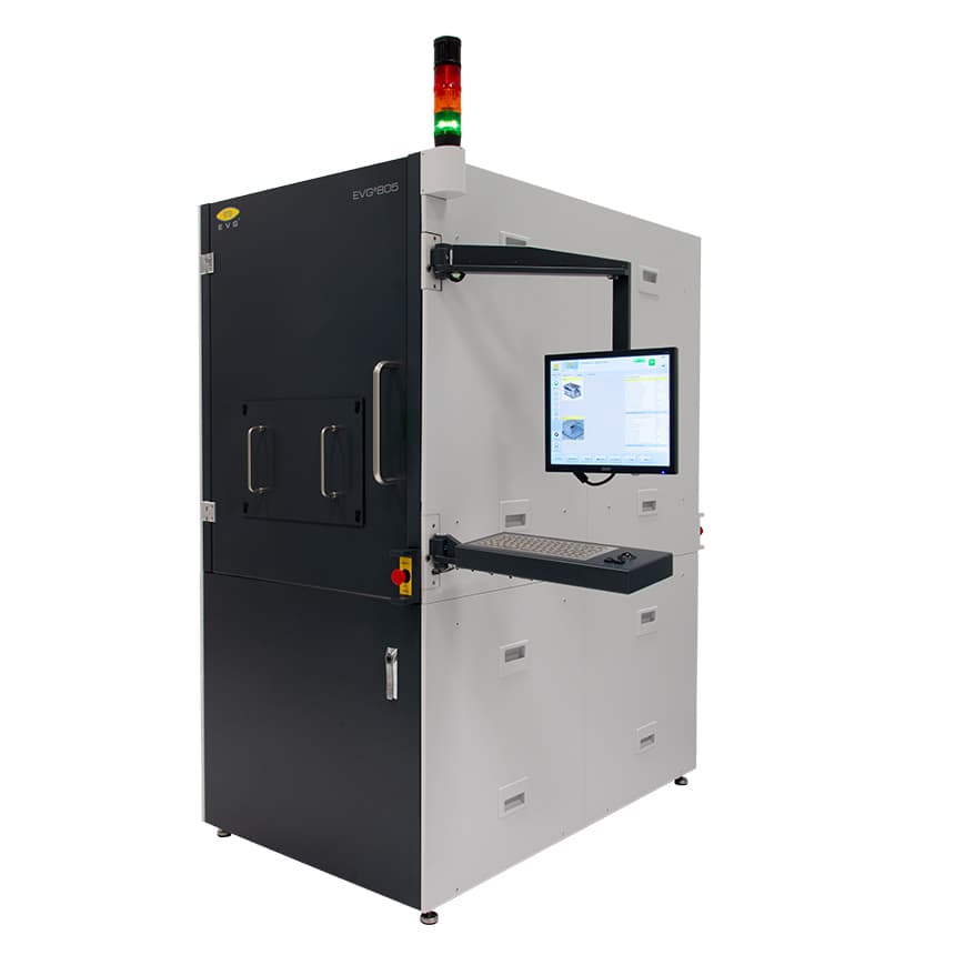
EVG®805
What is the EVG®805?
The EVG®805 is a specialised system for debonding temporarily bonded wafer stacks, which typically consist of a device wafer, a carrier wafer, and an intermediate temporary bonding adhesive.
IES is the official UK representative for EV Group (EVG), supplying, installing, and supporting the EVG®805 for customers across the UK.
What debonding processes does the EVG®805 support?
The EVG®805 supports both thermal and mechanical debonding processes, providing flexibility to match the specific temporary bonding adhesive and wafer stack in use.
What happens to the wafer after debonding?
Once debonded, the thin wafer is safely unloaded onto a single substrate carrier, ensuring reliable transport between tools and minimising handling risks to the fragile device wafer.
Where can I buy or get support for the EVG®805 in the UK?
As EV Group's official UK representative, IES provides UK-based sales, installation, and engineering support for the EVG®805 and the wider EVG temporary bonding portfolio.
Features:
- Open adhesive platform
- Debond Options:
- Thermal slide off debonding
- Lift off debonding
- Mechanical debonding
- Recipe controlled system
- Real time monitoring and recording of all relevant process parameters
- Unique features for thin-wafer handling
- Various chuck designs to support wafer/substrates and carriers up to 300 mm
- High topography wafer handling
Applications:
- 3D Integration / Through‑Silicon Via (TSV) Processing
In 3D IC fabrication, thinning the device wafer and performing back-side processing often requires mechanical support by bonding to a carrier. After the steps, debonding is critical. The EVG 805 provides controlled debonding. - Power Devices / Compound Semiconductors
For power or wide bandgap devices, thinning to reduce resistance is common. Temporary bonding followed by debonding is often used. - Advanced Packaging / Fan-out / Wafer-level Processing
When dies/substrates need backside steps or handling after thinning, temporary bonding + debonding is part of the process chain. - MEMS Devices
MEMS often include thin or delicate membranes; temporary bonding helps during processing, and safe debonding is needed after. - Process Development / R&D
In research fabs and development labs exploring new bonding adhesives, debonding chemistries, and workflows, a flexible debonding tool like EVG 805 is important.