


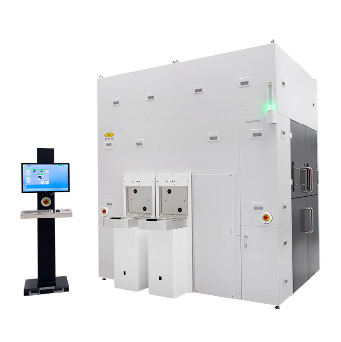
EVG®320
The EVG®320 is an automated single wafer cleaning system that handles wafers and substrates automatically between process stations. Equipped with a robotic handling system, it ensures precise pre-alignment and loading of wafers, supporting both cassette-to-cassette and FOUP-to-FOUP operations.
Features:
- Up to four cleaning stations
- Fully automated cassette-to-cassette or FOUP-to-FOUP handling
- Edge handling for double-sided cleaning processes available (option)
- High-efficiency cleaning using 1 MHz megasonic nozzles or area transducers (option)
- Advanced remote diagnostics
- Prevents cross-contamination from back to front side
- Fully software controlled cleaning process
Technical Data:
Wafer diameter (substrate size) - 200, 100 - 300 mm
Cleaning system
- Open chamber, spinner and cleaning arm
- Chamber: made of PP or PFA (option)
- Cleaning media: DI-water (standard), other cleaning media (option)
- Spinner chuck: vacuum chuck (standard) and edge handling chuck (option) made of metal ion free and clean materials
- Rotation: up to 3000 rpm (in 5 sec)
Megasonic nozzle
- Frequency: 1 MHz (3 MHz option)
- Output power: 30 - 60 W
- DI-water flow rate: up to 1.5 liter/min
- Effective cleaning area: Ø 4.0 mm
- Material: PTFE
Applications:
- Pre-Bonding Cleaning: Essential for preparing wafers before bonding processes such as fusion or hybrid bonding, ensuring surfaces are free from contaminants.
- Post-Debonding Cleaning: Used to remove residual bonding materials after debonding processes, preparing wafers for reuse or further processing.
- Advanced Packaging and 3D Integration: Supports applications requiring high cleanliness standards, such as 3D system-on-chip (SoC) devices and advanced packaging solutions.
- MEMS and Semiconductor Device Fabrication: Plays a crucial role in the fabrication of microelectromechanical systems (MEMS) and semiconductor devices, where surface cleanliness is critical for device performance and reliability.