- Equipment Partners
- Products
- EV Group
- Bonding
- ComBond
ComBond
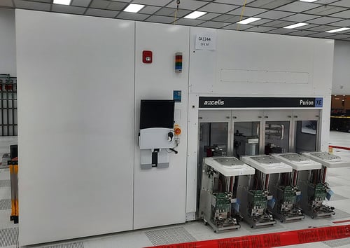
The EVG® ComBond high-vacuum wafer bonding platform sets a new standard in EVG’s portfolio, designed to meet the growing demand for advanced integration processes. Ideal for a wide range of applications, including engineered substrates, stacked solar cells, power devices, high-end MEMS packaging, and beyond CMOS technologies, the EVG® ComBond addresses the most sophisticated bonding needs. Its modular cluster design offers exceptional flexibility, enabling customization for both R&D and high-throughput, high-volume manufacturing environments. The platform excels in bonding heterogeneous materials with different lattice constants and coefficients of thermal expansion (CTE), while its unique oxide-removal process enables the formation of electrically conductive bond interfaces. The high-vacuum technology of the EVG® ComBond also supports low-temperature bonding of metals, such as aluminum, which re-oxidize quickly in ambient environments. Void-free and particle free bond interfaces, along with exceptional bond strength, can be achieved for a broad range of material combinations, making it an ideal solution for advanced device fabrication.
Features:
- High-vacuum, aligned, covalent bonding
- Processing in high-vacuum environment (< 5·10-8 mbar)
- In-situ sub-micron face-to-face alignment accuracy
- High-vacuum MEMS and optical device encapsulation
- In-situ surface and native oxide removal
- Superior surface properties
- Conductive bonding
- Room-temperature process
- Multiple material combinations, including metals (aluminum)
- Stress-free bond interface
- High bond strength
- Modular system for HVM and R&D
- Flexible configurations up to six modules
- Substrate size up to 200 mm
- Fully automated
Applications:
- “Beyond CMOS” / advanced logic / high-mobility devices
When integrating different semiconductor materials (e.g. III-V on Si), oxide-free bonding via ComBond helps maintain high interface quality. - MEMS / vacuum-sealed MEMS devices
For MEMS requiring vacuum encapsulation (gyroscopes, accelerometers, microbolometers, etc.), ComBond can bond capping wafers under vacuum and maintain high vacuum environments inside. - Power / high-voltage / power electronics
Bonding wide bandgap materials, or bonding heterogenous materials (e.g. SiC, GaN) with minimal thermal damage and strong interfaces, is possible with ComBond.
Book a Live or Virtual Demo
See the capabilities of our partners' equipment - including EVG, scia Systems, Veeco, PPS and SSI - in action. Experience tailored demonstrations designed around your process and application needs.


