




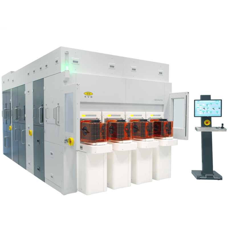
GEMINI FB XT
What is the GEMINI® FB XT?
Vertical stacking of semiconductor devices is an increasingly effective approach to advancing device density and performance, and wafer-to-wafer bonding is a critical process enabling 3D stacked devices. The EVG® GEMINI FB XT is an integrated fusion bonding system that extends current standards, combining higher productivity with improved alignment and overlay accuracy.
IES is the official UK representative for EV Group (EVG), supplying, installing, and supporting the GEMINI FB XT for customers across the UK.
What alignment technology does it use?
The GEMINI FB XT is equipped with the SmartView® NT3 face-to-face bond aligner, delivering sub-50 nm wafer-to-wafer alignment accuracy — purpose-built to meet the demanding requirements of fusion and hybrid wafer bonding alignment.
How is the system configured for production?
The GEMINI FB XT supports up to six pre-processing modules, including clean, LowTemp™ plasma activation, alignment verification, and debond modules, and uses an XT Frame concept with an EFEM (Equipment Front End Module) for maximum throughput. Optional features include a thermocompression bond module.
What applications is it used for?
The GEMINI FB XT is ideal for applications such as memory stacking, 3D systems on chip (SoC), backside illuminated CMOS image sensor stacking, and die partitioning.
Where can I buy or get support for the GEMINI FB XT in the UK?
As EV Group's official UK representative, IES provides UK-based sales, installation, and engineering support for the GEMINI FB XT and the wider EVG bonding equipment portfolio.
Features:
- New SmartView® NT3 face-to-face bond aligner with sub 50 nm wafer-to-wafer alignment accuracy
- Up to six pre-processing modules like:
- Clean module LowTemp™ plasma activation module
- Alignment verification module
- Debond module XT Frame concept for highest throughput with EFEM (Equipment Frontend Module)
- Optional features:
- Debond module
- Thermocompression bond module
Applications:
- Memory Stacking
The GEMINI® FB is utilized in stacking memory devices, enabling increased storage capacity and improved performance in semiconductor products. - 3D Systems on Chip (SoC)
It supports the integration of multiple functional layers into a single chip, enhancing device functionality and reducing form factor. - Backside Illuminated (BSI) CMOS Image Sensors
The system is employed in bonding processes for BSI CMOS image sensors, which are crucial for high-performance imaging applications. - Die Partitioning
It facilitates die partitioning, allowing for the separation of large die into smaller functional units, optimizing manufacturing processes. - Collective Die-to-Wafer (Co-D2W) Bonding
The GEMINI® FB is configured for Co-D2W bonding, enabling the transfer of multiple dies onto a wafer in a single process step, enhancing throughput and efficiency.