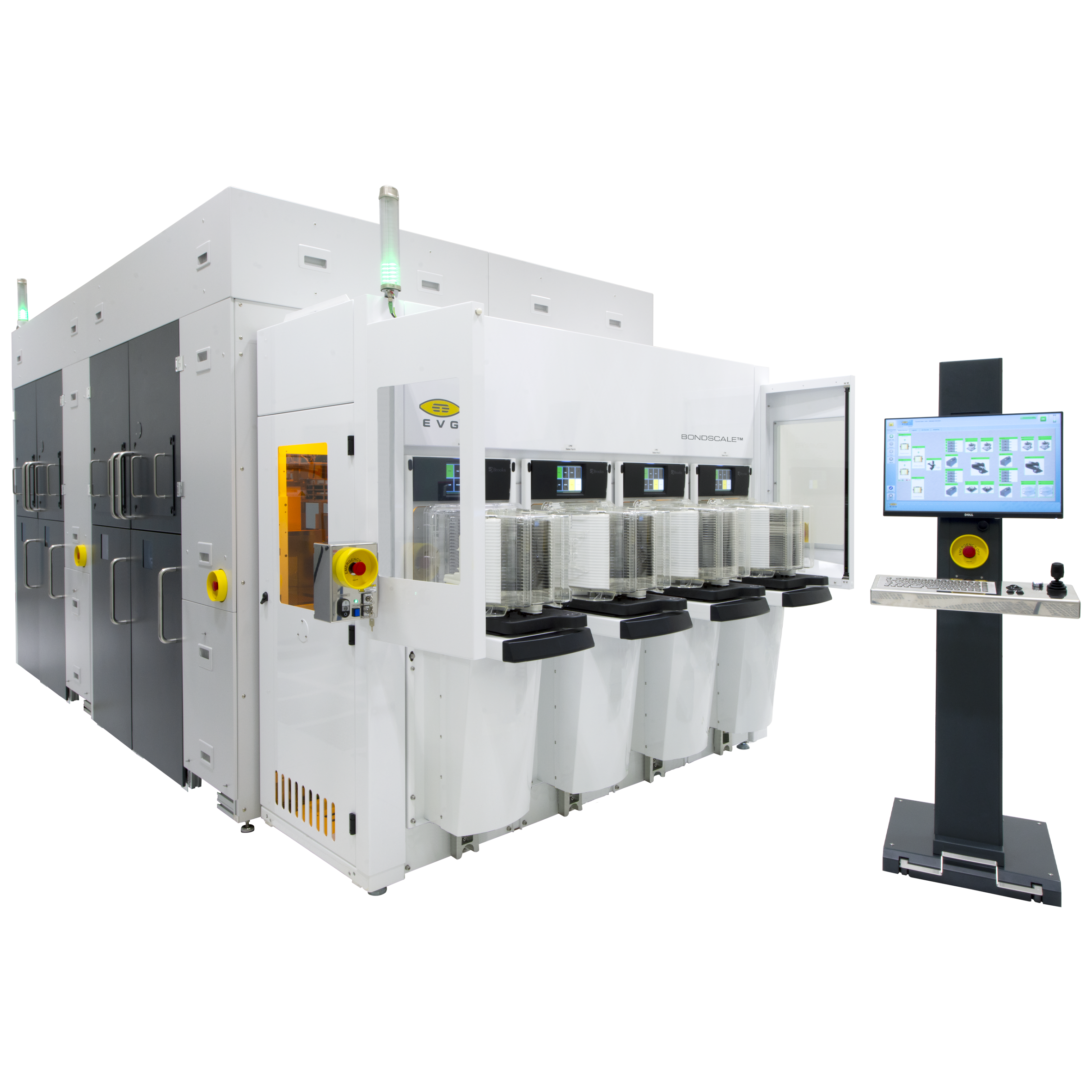
BONDSCALE
EVG BONDSCALE fulfils a broad variety of applications for fusion and molecular wafer bonding, including 3D integration approaches (e.g. monolithic 3D) which employ layer transfer processing and engineered substrate manufacturing. BONDSCALE incorporates heightened edge alignment technology, enabling a major boost in productivity and bringing down cost of ownership relative to alternative fusion bonding platforms on the market.
The GEMINI FB XT automated fusion bonding system - considered an industry benchmark - is typically sold with BONDSCALE, encompassing a range of different applications. GEMINI FB XT supports applications necessitating high alignment accuracies like backside illuminated CMOS image sensor stacking, 3D systems on chip (SoC), memory stacking and die partitioning.
BONDSCALE is enabling EVG to bring wafer bonding to front end semiconductor processing. Significantly, is also addressing challenges outlined in the International Roadmap for Devices and Systems (IRDS).
Features
- Fully automated fusion/molecular wafer bonding applications on 200 mm and 300 mm substrates in a single platform
- Direct wafer bonding with plasma activation for heterogeneous integration of different materials, high-quality engineered substrates as well as thin-silicon layer-transfer applications
- Layer-transfer processes and engineered substrates enabling logic scaling, 3D integration such as M3, 3D VLSI including backside power distribution, N&P stacking, logic-on-memory, clustered functional stacks and beyond-CMOS adoption