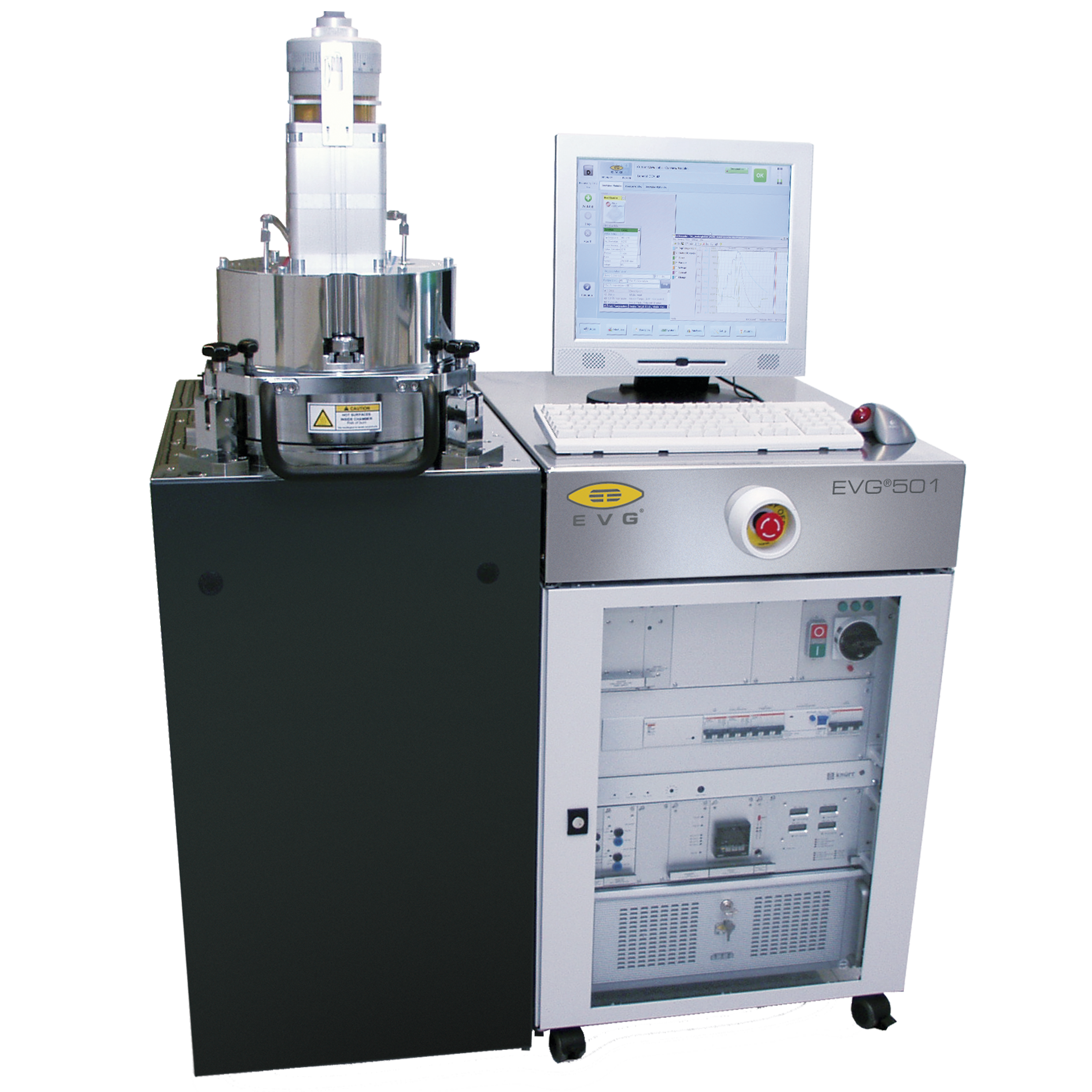
EVG®501
The EVG501 is a highly adaptable wafer bonding system which is capable of handling substrate sizes from single chips up to 150 mm, or 200 mm for 200 mm bond chambers. Every standard bonding process is supported by the tool, including anodic, solder, transient liquid phase, direct and glass frit and eutectic.
A conversion time of under five minutes is made possible by simplified retooling for various wafer sizes and processes, which is afforded by the EVG501’s tooling design and easily accessible bond chamber. The EVG501’s bond chamber design is identical to those used in the EVG Gemini and its other tools for high volume manufacturing. This adaptability can make the EVG501 suitable for R&D facilities and universities, as well as low volume production facilities. The tool facilitates easily transferable bonding recipes which are conducive to easy production volume scale up.
Features
- Unique pressure and temperature uniformity
- Compatible with EVG mechanical and optical aligners
- Flexible design and configurations for research
- From single chips to wafers
- Various processes (eutectic, solder, TLP, direct bonding)
- Optional turbopump (<1E-5mbar)
- Upgradeable for anodic bonding
- Open chamber design for easy conversion and maintenance
- Pilot production compatible
- Open chamber design for easy conversion and maintenance
- Smallest footprint for a 200 mm bonding system: 0.8 m2
- Recipes are fully compatible with EVG’s high-volume-manufacturing bonding systems